PCBA appearance detection method and device

A technology of appearance inspection and inspection method, applied in the field of PCBA appearance inspection method and device, can solve the problem of incompatibility of PCB inspection method, and achieve the effects of low cost, improved inspection efficiency, and simple device structure

Pending Publication Date: 2022-02-01
HRG INT INST FOR RES & INNOVATION
View PDF1 Cites 2 Cited by
  • Summary
  • Abstract
  • Description
  • Claims
  • Application Information

AI Technical Summary

Problems solved by technology

[0005] Although the above-mentioned prior art has the advantages of fast, accurate, reliable, etc., which can speed up the detection speed of circuit board components, however, for PCBA, there are three-dimensional electronic components of different specifications installed on the surface, and the situation of installation inclination is relatively common, resulting in the traditional PCB detection methods are difficult to be compatible

Method used


Image

  • PCBA appearance detection method and device
  • PCBA appearance detection method and device
  • PCBA appearance detection method and device

Examples


Embodiment

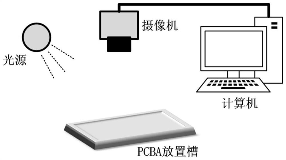
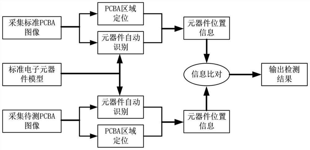
[0035] Such as figure 1 As shown, a PCBA board appearance detection device includes: a computer, a camera, a light source, and a PCBA placement groove, the camera is connected to the computer, the PCBA placement groove is used to place the PCBA board, and the light source is installed on the PCBA The top of the placement slot is used for system lighting; the field of view of the camera can cover the PCBA placement slot, and the light source irradiation area also needs to cover the PCBA placement slot, and the light intensity distribution is relatively uniform; the slot size of the PCBA placement slot and the appearance size of the PCBA Equal, the PCBA board can be placed in the PCBA placement slot just to ensure that the placement position and posture of the PCBA are consistent each time, so the area of ​​interest in the image is less offset; at the same time, the appearance color of the PCBA placement slot is single, and There is a large color difference with the color of the...


PUM


Abstract

The invention discloses a PCBA appearance detection method and device, belongs to the technical field of industrial visual detection, and solves the problem of how to improve the detection efficiency of a PCBA of which the surface is provided with complex three-dimensional electronic components by adopting a machine visual detection method. The method comprises the following steps of: applying a component model obtained by deep learning training to a standard PCBA image, and extracting and identifying each component in the standard PCBA image; comparing the position information of the components of the to-be-detected PCBA board with the position information of the components of a standard PCBA board one by one, calculating the area cross ratio IOU of each corresponding marking frame to judge whether wrong welding and missing welding exist in electronic components or not, and the problems that due to the fact that a manual visual mode is mainly adopted in traditional PCBA appearance detection, the labor intensity is high, workers are prone to fatigue, and the detection efficiency is low are solved, the labor cost is reduced, and the detection efficiency is improved; the device is simple in structure and low in cost.

Description

technical field [0001] The invention belongs to the technical field of industrial visual inspection, and relates to a PCBA appearance inspection method and device. Background technique [0002] PCBA (Printed Circuit Board Assembly), which refers to the finished printed circuit board made of PCB printed circuit board through SMT (Surface Mounted Technology) patch or DIP (Dual In-line Package) plug-in, has been widely used in various electronic products, covering Communication networks, household appliances, industrial control, consumer electronics, medical electronics, aerospace and other fields. [0003] With the development of electronic products in the direction of low power consumption, light weight, and intelligence, the assembly density and integration of printed boards are getting higher and higher, so PCBA appearance inspection is very important. The traditional PCBA appearance inspection mainly uses manual visual inspection to detect whether there are problems such ...

Claims


Application Information

Patent Timeline
Patent Type & Authority Applications(China)
IPC IPC(8): G06T7/00G06T7/136G06T7/73G06T7/62G06N3/04G06N3/08G01N21/88
CPCG06T7/0006G06T7/136G06T7/73G06T7/62G06N3/04G06N3/08G01N21/8851G06T2207/30141G01N2021/8887
Inventor 李文兴顾文庆蒋忠胜于振中
Owner HRG INT INST FOR RES & INNOVATION
Why Eureka
Try Eureka