Optical device integrated circuit structure and assembly method

A circuit structure and optical device technology, applied in the field of optical communication, can solve the problems of impedance return loss, poor transmission effect, impedance discontinuity, etc.

Pending Publication Date: 2022-02-08
WUHAN OPTICAL VALLEY INFORMATION OPTOELECTRONICS INNOVATION CENT CO LTD
View PDF9 Cites 1 Cited by
  • Summary
  • Abstract
  • Description
  • Claims
  • Application Information

AI Technical Summary

Problems solved by technology

[0003] In high-frequency or high-bandwidth applications, under normal circumstances, the impedance requirement of the gold wire bond is 50 ohms, but the impedance is affected by factors such as the diameter of the bonded gold wire, the lin

Method used


Image

  • Optical device integrated circuit structure and assembly method
  • Optical device integrated circuit structure and assembly method
  • Optical device integrated circuit structure and assembly method

Examples


Embodiment Construction

[0036] It should be noted that, in the case of no conflict, the embodiments in the present application and the technical features in the embodiments can be combined with each other, and the detailed description in the specific embodiment should be understood as an explanation of the present application, and should not be regarded as an explanation of the present application. Undue Restriction of Application.

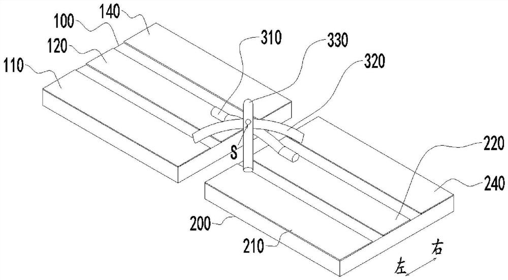
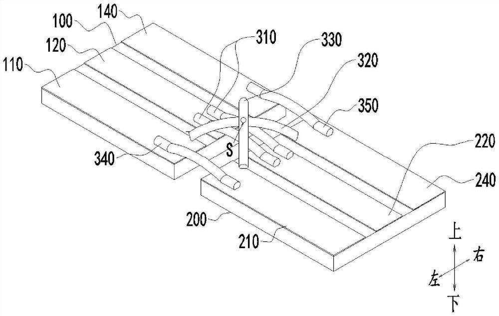
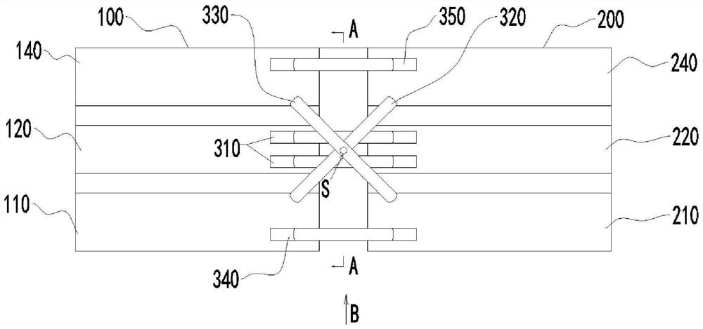
[0037] In the description of the embodiments of this application, the orientations or positional relationships of "upper", "lower", "left", "right", "front", "back" are based on the attached figure 2 It should be understood that these orientation terms are only for the convenience of describing the application and simplifying the description, rather than indicating or implying that the referred device or element must have a specific orientation, be configured in a specific orientation, and operation and therefore should not be construed as limiting the application.

[...


PUM


Abstract

The embodiment of the invention discloses an optical device integrated circuit structure and an assembly method, and the circuit structure comprises a first coplanar waveguide unit which comprises a first grounding strip, a first signal strip and a second grounding strip which are sequentially arranged from left to right; a second coplanar waveguide unit and the first coplanar waveguide unit are arranged at an interval, and the second coplanar waveguide unit comprises a third grounding strip, a third signal strip and a fourth grounding strip which are sequentially arranged from left to right; a first bonding wire is connected between the first signal strip and the third signal strip; a second bonding wire is connected between the first grounding strip and the fourth grounding strip; a third bonding wire is connected between the second grounding strip and the third grounding strip; and the second bonding wire and the third bonding wire intersect to form an intersection point S located above the first bonding wire. The embodiment of the invention has the advantage of good impedance continuity.

Description

technical field [0001] The present application relates to the field of optical communication, in particular to an integrated circuit structure and assembly method of optical devices. Background technique [0002] In the field of optical communication, the circuit structure of optical device integration is usually connected by gold wire bonding, and the gold wires used in gold wire bonding have their fixed specifications and sizes, and cannot be adjusted like traveling wave electrodes or transmission lines. Line width and other parameters to achieve impedance matching. [0003] In high-frequency or high-bandwidth applications, under normal circumstances, the impedance requirement of the gold wire bond is 50 ohms, but the impedance is affected by factors such as the diameter of the bonded gold wire, the line distance, and the dielectric constant of the air. The impact is usually much greater than 50 ohms, resulting in discontinuous impedance, resulting in impedance mismatch t...

Claims


Application Information

Patent Timeline
IPC IPC(8): G02B6/42
CPCG02B6/4279
Inventor 王桂晨傅焰峰王栋严杰
Owner WUHAN OPTICAL VALLEY INFORMATION OPTOELECTRONICS INNOVATION CENT CO LTD
Why Eureka
Try Eureka