Optical detector and preparation method thereof

A photodetector, photodetection technology, applied in the direction of photometry using electrical radiation detectors, semiconductor devices, final product manufacturing, etc., can solve the lack of second-order nonlinear optical effects and linear electro-optical effects, second-order nonlinear devices And the disadvantages of electro-optical modulators, the difficulty of preparation technology, etc., to achieve the effect of shortening detection time, good applicability, and improving accuracy

Pending Publication Date: 2022-02-08
上海新硅聚合半导体有限公司
View PDF0 Cites 1 Cited by
  • Summary
  • Abstract
  • Description
  • Claims
  • Application Information

AI Technical Summary

Problems solved by technology

[0003] However, silicon also has limitations brought by its own material: 1. Silicon is a centrosymmetric crystal material, so it lacks second-order nonlinear optical effects and linear electro-optic effects, so it faces difficulties in preparing second-order nonlinear devices and electro-optic modulators. natural disadvantage
2. The intrinsic absorption edge of silicon material is around 1100nm, and the commonly used bands of integrated optics, 1310nm and 1550nm, are transparent to silicon, so it is necessary to integrate other materials on silicon, such as Ge, for light detection, which greatly improves the technical difficulty
[0004] Therefore, there is an urgent need for a technical solution for photodetectors to solve the problems of traditional detectors, such as difficult preparation technology, long detection time, and the need to integrate multiple materials to increase the integration difficulty.

Method used


Image

  • Optical detector and preparation method thereof
  • Optical detector and preparation method thereof
  • Optical detector and preparation method thereof

Examples


Embodiment Construction

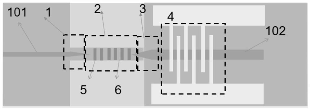
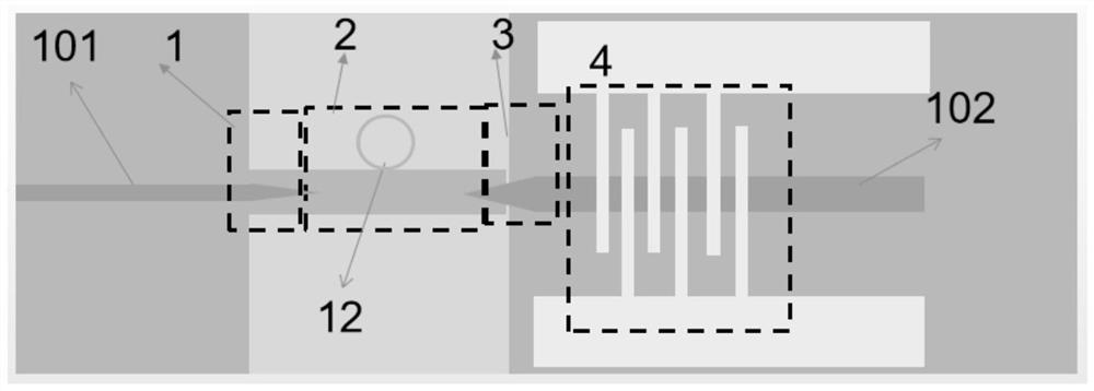
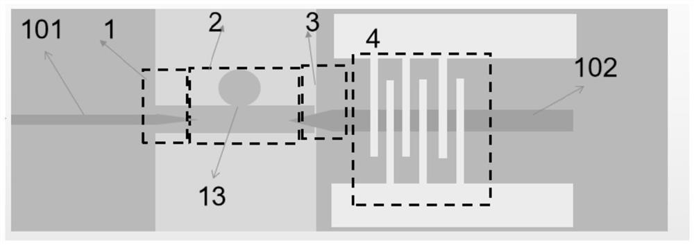
[0042] The following will clearly and completely describe the technical solutions in the embodiments of the application with reference to the drawings in the embodiments of the application. Apparently, the described embodiments are only some of the embodiments of the application, not all of them. Based on the embodiments in the present application, all other embodiments obtained by persons of ordinary skill in the art without making creative efforts belong to the protection scope of the present application.

[0043] It should be noted that, in the description of the creation of the present application, the terms "comprising" and "having" and any variations thereof are intended to cover non-exclusive inclusion, for example, processes, methods, and systems that include a series of steps or units The process, method, product or device are not necessarily limited to those steps or units explicitly listed, but may include other steps or units not explicitly listed or inherent to the...


PUM

PropertyMeasurementUnit
Wavelengthaaaaaaaaaa

Abstract

The invention discloses an optical detector and a preparation method thereof. The optical detector comprises a first transmission waveguide, a second transmission waveguide, a first coupler, a second coupler, a wavelength converter and an optical detection structure, wherein the first coupler is arranged between the first transmission waveguide and the wavelength converter, and the first coupler can make the first transmission waveguide and the wavelength converter conduct light conduction; the wavelength converter is used for performing wavelength conversion on the optical signal output by the first coupler; the second coupler is arranged between the second transmission waveguide and the wavelength converter, and the second coupler can make the second transmission waveguide and the wavelength converter conduct light conduction; the light detection structure is used for detecting light signals output by the second coupler, light in a transparent wave band for a silicon material is converted into light in a non-transparent wave band through the prepared light detector, and then the light is detected, so that the detection precision is improved, other materials are prevented from being integrated to prepare the detector, the difficulty of the preparation technology is also reduced, and the production cost is reduced.

Description

technical field [0001] The present application relates to the technical field of preparation and application of photodetectors, in particular to a photodetector and a preparation method thereof. Background technique [0002] With the progress of the times, the huge application potential of integrated optics in optical interconnection, optical computing, etc. CMOS process technology enables large-scale fabrication. [0003] However, silicon also has limitations brought by its own material: 1. Silicon is a centrosymmetric crystal material, so it lacks second-order nonlinear optical effects and linear electro-optic effects, so it faces difficulties in preparing second-order nonlinear devices and electro-optic modulators. With natural disadvantages. 2. The intrinsic absorption edge of silicon material is around 1100nm, and the commonly used bands of integrated optics, 1310nm and 1550nm, are transparent to silicon, so it is necessary to integrate other materials on silicon, suc...

Claims


Application Information

Patent Timeline
IPC IPC(8): H01L31/0232H01L31/105H01L31/108H01L31/18G01J1/42
CPCH01L31/105H01L31/1085H01L31/18H01L31/02327H01L31/1804G01J1/42Y02P70/50
Inventor 欧欣陈阳黄凯
Owner 上海新硅聚合半导体有限公司
Why Eureka
Try Eureka