Full-color Micro-LED display panel and manufacturing method thereof

A display panel, full-color technology, applied in the direction of semiconductor devices, electrical components, circuits, etc., can solve the problems that affect the display contrast, color purity and saturation, crosstalk, and affect the image quality of full-color Micro-LED display, etc. Achieve the effects of improving processing efficiency, meeting high-precision requirements, and solving luminous crosstalk

Pending Publication Date: 2022-02-08
WUHAN UNIV
View PDF0 Cites 0 Cited by
  • Summary
  • Abstract
  • Description
  • Claims
  • Application Information

AI Technical Summary

Problems solved by technology

In the full-color display of the three primary colors of red, green and blue, the light emitted from the side wall of the Micro-LED chip will crosstalk to adjacent chips, affecting the contrast, color purity and saturation of the display
Seriously affect the image quality of full-color Micro-LED display

Method used


Image

  • Full-color Micro-LED display panel and manufacturing method thereof
  • Full-color Micro-LED display panel and manufacturing method thereof
  • Full-color Micro-LED display panel and manufacturing method thereof

Examples


Embodiment 1

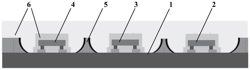
[0043] Embodiment 1 provides a full-color Micro-LED display panel, including: a driver panel, a three-primary-color Micro-LED chip array, a curved reflector array, and packaging glue; the three-primary-color Micro-LED chip array, the curved surface reflection The mirror arrays are all placed on the drive panel; the three primary color Micro-LED chip arrays include several flip-chip red Micro-LED chips, flip-chip green Micro-LED chips and flip-chip blue Micro-LED chips; The curved reflector array includes several curved reflectors, and several curved reflectors form a cavity array, and a reflective layer is deposited on the inner wall of the cavity array; Red Micro-LED chip, the flip-chip green Micro-LED chip and the flip-chip blue Micro-LED chip; the encapsulation glue is filled in the cavity array, and the encapsulation glue covers the Micro-LED chip and the curved mirror.

[0044] The DBR reflective layer in the flip-chip red Micro-LED chip, the flip-chip green Micro-LED ch...

Embodiment 2

[0064] Embodiment 2 provides a method for preparing the Micro-LED display chip as described in Embodiment 1, comprising the following steps:

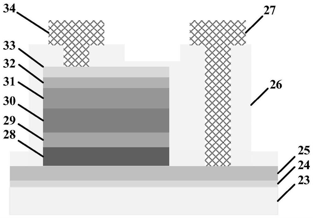
[0065] Step 1. Obtain flip-chip red Micro-LED chips, flip-chip green Micro-LED chips, and flip-chip blue Micro-LED chips with complete structures.

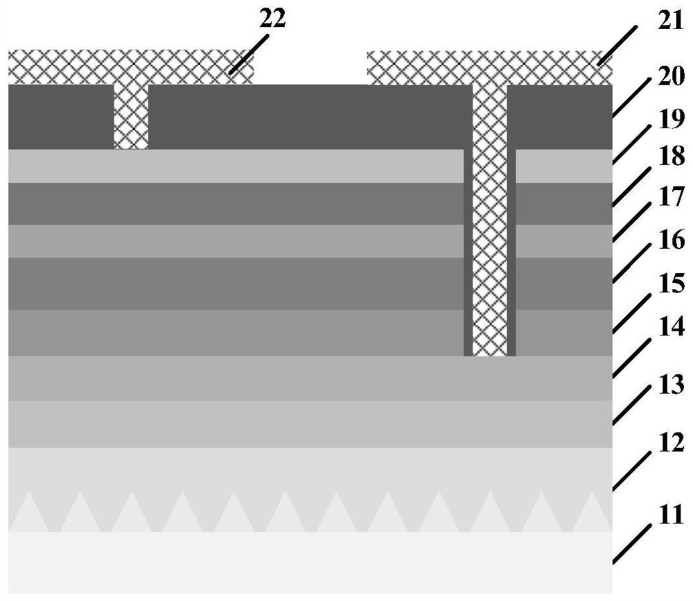
[0066] Obtain flip-chip red, green, and blue Micro-LED chips with a complete structure, specifically from epitaxial growth to p- / n-electrode deposition and other complete Micro-LED chip structures. The length of each chip is 30-60 microns, and the width It is 30-60 microns, and the thickness is 8-10 microns.

[0067] Step 2. Bond the three primary color flip-chip Micro-LED chips (the flip-chip red Micro-LED chip, the flip-chip green Micro-LED chip and the flip-chip blue Micro-LED chip) to the driver panel in sequence Above, a three-color Micro-LED chip array is formed; the lateral distance between two adjacent Micro-LED chips is greater than the chip length, and the vertical distance betwe...


PUM

PropertyMeasurementUnit
thicknessaaaaaaaaaa
thicknessaaaaaaaaaa
reflectanceaaaaaaaaaa

Abstract

The invention belongs to the technical field of semiconductor light-emitting devices, and discloses a full-color Micro-LED display panel and a manufacturing method thereof. A three-primary-color Micro-LED chip array and a curved-surface reflector array are both arranged on a driving panel, a plurality of curved-surface reflectors form a cavity array, a reflecting layer is deposited on the inner wall of the cavity array, inverted red-light, green-light and blue-light Micro-LED chips are sequentially arranged in the cavity array, the cavity array is filled with packaging glue, and the packaging glue covers the Micro-LED chips and the curved-surface reflectors. According to the invention, the crosstalk phenomenon between the adjacent Micro-LED chips can be reduced, and the image quality of the full-color Micro-LED display panel is remarkably improved.

Description

technical field [0001] The invention belongs to the technical field of semiconductor light emitting devices, and more specifically relates to a full-color Micro-LED display panel and a manufacturing method thereof. Background technique [0002] Group-III nitride light-emitting diodes (Light Emitting Diodes, referred to as "LEDs") are made of single-crystal compound semiconductors because of their higher luminous efficiency and higher Strong durability, widely used in display applications such as lighting, digital signage, and LCD backlighting. In recent years, in the display industry, there has been an increasing demand for self-luminous displays with very wide color gamut and high resolution, and micro-light-emitting diodes (Micro-LEDs) are considered to be the best for realizing high-resolution and wide color gamut displays. It has the characteristics of low power consumption, fast response, long life and high light efficiency. [0003] As the size of the Micro-LED chip ...

Claims


Application Information

Patent Timeline
Patent Type & Authority Applications(China)
IPC IPC(8): H01L33/60H01L25/075
CPCH01L33/60H01L25/0753H01L2933/0058
Inventor 周圣军施浪杜鹏
Owner WUHAN UNIV
Why Eureka
Try Eureka