
Modulator chip assembly for high rate optical signal generation

A high-speed signal and modulator technology, used in laser parts, lasers, semiconductor lasers, etc., can solve the problem of insufficient 50Gb/s signal modulation, and achieve the effect of ensuring mass production, realizing bandwidth, and overcoming bandwidth limitations.

Pending Publication Date: 2022-02-11
欧润光电科技(苏州)有限公司
View PDF0 Cites 0 Cited by
  • Summary
  • Abstract
  • Description
  • Claims
  • Application Information

AI Technical Summary

Problems solved by technology

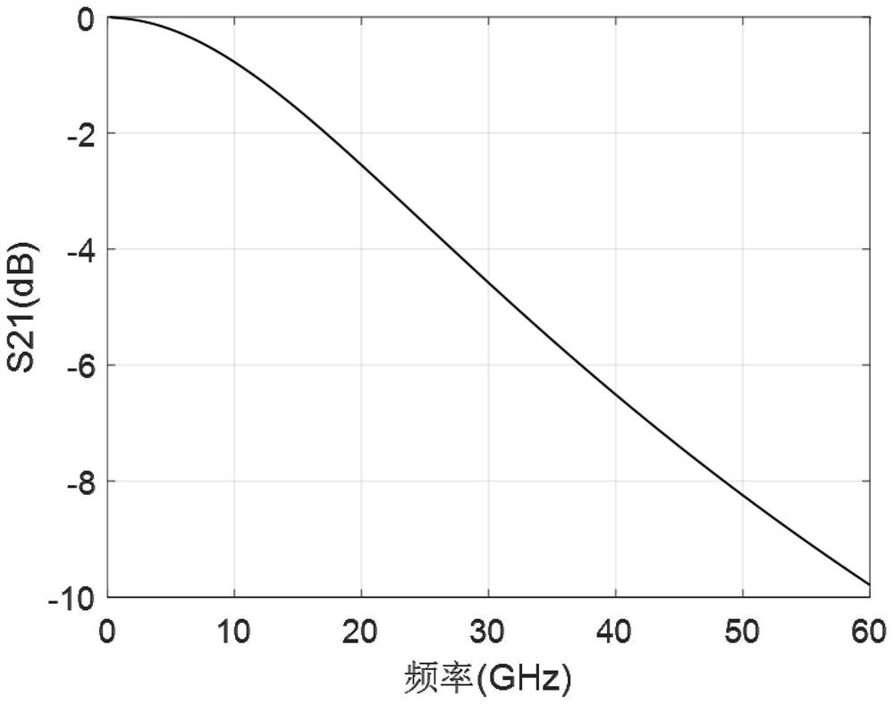
Although the bandwidth of the modulator can be increased from 22.4GHz to about 33GHz by introducing an inductor, it is generally required that the 3dB bandwidth of the modulator should be above 35GHz to modulate a 50Gb / s signal, so the modulator’s intrinsic bandwidth of 22GHz is only Adding inductance is still not enough to guarantee the modulation of 50Gb / s signal

Method used


Image

  • Modulator chip assembly for high rate optical signal generation
  • Modulator chip assembly for high rate optical signal generation
  • Modulator chip assembly for high rate optical signal generation

Examples


Embodiment 1

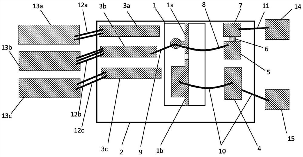
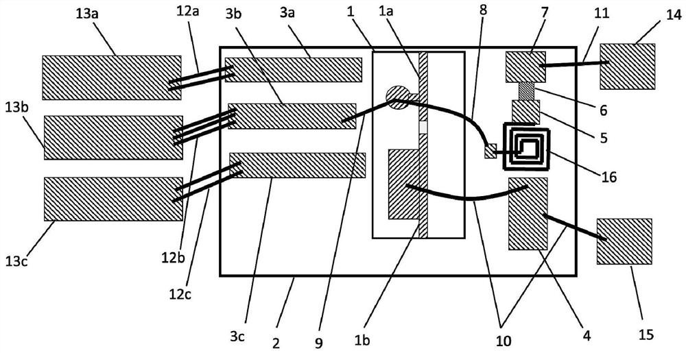
[0066] Such as Figure 5 As shown, the modulator chip assembly used for high-speed optical signal generation in the present invention includes an electroabsorption modulation laser 1, a capacitor 17, a second inductance 16, a first inductance 18, and a matching resistor 6; wherein the electroabsorption modulation laser 1 includes an electroabsorption modulator 1a and a semiconductor laser 1b. A high-speed electrical signal is applied to the electroabsorption modulator 1a to modulate the DC light emitted by the semiconductor laser 1b to generate a high-speed optical signal output; all these components (including the electroabsorption modulation laser 1, capacitor 17 , the second inductor 16, the first inductor 18 and the matching resistor 6) are all located on the same substrate 2;

[0067] The substrate 2 also includes a plurality of microwave transmission lines and electrodes for connecting external circuits and electroabsorption modulated lasers, and resistors 6 (generally 5...

Embodiment 2

[0082] Such as Figure 12 As shown, the first inductor 18 that was originally located on the same substrate 2 as the capacitor 17 is replaced by a first gold wire 91 of a certain length; the first gold wire 91 not only provides the connection between the signal line 3b and the modulator chip 1a, but also acts as the first inductor 18. Compared with Embodiment 1, Embodiment 2 replaces the first inductor 18 with a gold wire, which can not only reduce the cost, but also because the length of the gold wire can be adjusted during chip packaging, and the inductance value also changes accordingly, so gold wires of different lengths The wire will be able to function as an adjustable inductance. Since the parameters of modulator chips from different suppliers are different, adjusting the inductance value by changing the length of the first gold wire 91 will greatly facilitate the adjustment of resonance characteristics for different modulator chips to obtain the best response performa...

Embodiment 3

[0084] Going a step further, as in Figure 13 As shown, the first inductor 18 originally located on the same substrate 2 as the capacitor 17 is replaced by a first gold wire 92 of a certain length, and the second inductor 16 is replaced by a second gold wire 82 . The first gold wire 92 not only provides the connection between the signal wire 3 b and the modulator chip 1 a, but also acts as the first inductor 18 , and the second gold wire 82 acts as the second inductor 16 . Compared with Embodiment 1, Embodiment 3 replaces the first inductance 18 and the second inductance 16 with two first gold wires 92 and second gold wires 82 of different lengths, which not only can further reduce the cost, but also because the length of the gold wires It can be adjusted when the chip is packaged, and the inductance value will also change accordingly, so gold wires of different lengths will be able to play the role of adjustable inductance. On the premise of considering the parasitic effect,...


PUM

PropertyMeasurementUnit
lengthaaaaaaaaaa
lengthaaaaaaaaaa
lengthaaaaaaaaaa

Abstract

The invention discloses a modulator chip assembly for generating a high-speed optical signal. The modulator chip assembly comprises a modulator chip, at least one high-speed signal transmission line, at least one ground wire, a capacitor, a resistor and at least two sections of gold wires, wherein the length of the first gold thread is L1, and L1 is larger than 0.05 mm and smaller than or equal to 1 mm, or the length L1 of the first gold thread is smaller than or equal to 0.05 mm. The modulator chip assembly also comprises a first inductor, wherein one end of the first inductor is connected with the first gold wire, and the other end of the first inductor is connected with the capacitor through the high-speed signal transmission line; the first inductor is located between the modulator chip and the capacitor; the first inductor is connected in series with the modulator chip. According to the low-bandwidth modulator, the shunt capacitor and the series inductor are added between the microwave signal line and the modulator chip to further improve the bandwidth of the modulator chip, so the low-bandwidth modulator can be applied to modulation of signals of 50G and above, and the bandwidth of the modulator chip assembly is conveniently increased at low cost.

Description

technical field [0001] The invention relates to a signal modulating device in the communication field, in particular to a modulator chip component used for high-speed optical signal generation. Background technique [0002] With the construction of large-scale data centers, 100G / 400G / 800G transmission technology has become inevitable. However, there are many challenges in the process of upgrading from traditional 10G networks to networks above 100G / 400G / 800G, one of which is the demand for high-bandwidth, low-cost modulator chips for high-speed optical signals. [0003] At present, the core modulation chip that realizes single-wavelength 100G and four-channel 400G transmission is a 50Gb / s semiconductor electroabsorption modulation laser. As a key chip for high-speed optical signal generation, the semiconductor electroabsorption modulator's bandwidth is mainly limited by the junction capacitance and parasitic capacitance of the chip. Therefore, to increase the modulation ba...

Claims


Application Information

Patent Timeline
Patent Type & Authority Applications(China)
IPC IPC(8): H04B10/50H04B10/556H01S5/026
CPCH04B10/504H04B10/5563H01S5/0261
Inventor 方祖捷王中和
Owner 欧润光电科技(苏州)有限公司
Learn More