Electrostatic protection device and manufacturing method thereof

A technology of electrostatic protection device and manufacturing method, which is applied in the semiconductor field, can solve problems such as false triggering of parasitic SCR, and achieve the effect of avoiding false triggering of latch phenomenon

Pending Publication Date: 2022-02-22
JOULWATT TECH INC LTD
View PDF0 Cites 0 Cited by
  • Summary
  • Abstract
  • Description
  • Claims
  • Application Information

AI Technical Summary

Problems solved by technology

[0005] The purpose of the present invention is to provide an electrostatic protection device and its manufacturing method, which can overcome the problem of false triggering of the parasitic SCR in the double-digit LDMOS-SCR device in the prior art when voltage overshoot or voltage spikes occur, resulting in deep hysteresis to Very low sustain voltage causes latch-up, i.e. avoid false triggering of latch-up

Method used


Image

  • Electrostatic protection device and manufacturing method thereof
  • Electrostatic protection device and manufacturing method thereof
  • Electrostatic protection device and manufacturing method thereof

Examples


Embodiment Construction

[0037] The present invention will be described in detail below, but it should be explained, and these embodiments are not intended to limit the functions, methods, or structural equivalent transformations or substitutions of these embodiments according to these embodiments. It is within the scope of the invention.

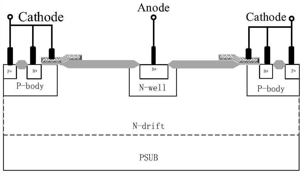
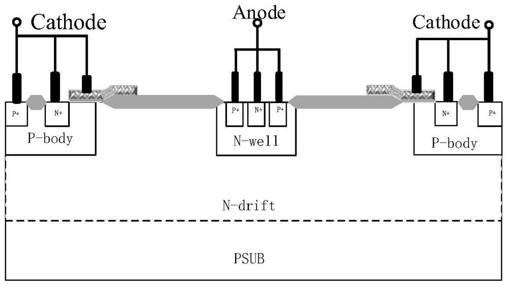
[0038] As described in the conventional LDMOS-SCR structure, it is prone to the latching effect, which is prone to the devices to be burned after misconcing. After the applicant has undergone this phenomenon, the principle of discovering the technical problem is as follows: For a traditional LDMOS-SCR structure, its equivalent circuit is like figure 2 As shown, two symmetric distributed MOS devices, wherein N-Well constitutes a drain region, and since a n-type retaining region is included in the drain region, a N-type diver is included, each MOS is included. The devices produce parasitic triode NPN and PNP. When the ESD pulse is in the ESD pulse, the positive voltage c...


PUM


Abstract

The invention provides an electrostatic protection device and a manufacturing method thereof. The electrostatic protection device comprises: a substrate; a drift region formed on the substrate; a well region formed on the drift region; and a first body region and a second body region which are arranged on the two sides of the well region respectively, wherein the distance between the well region and the first body region is smaller than the distance between the well region and the second body region. Only a first heavily doped region is arranged in the first body region, a second heavily doped region and a third heavily doped region are arranged in the second body region, and only a fourth heavily doped region is arranged in the well region. Only a parasitic PNP triode is reserved on one side of the drain end of a traditional LDMOS-SCR device, a parasitic SCR is reserved on the other side of the drain end of the traditional LDMOS-SCR device, meanwhile, the relevant size is designed, so thateffective electrostatic protection is achieved, and the PNP is triggered before the SCR, and the latch-up phenomenon caused by deep hysteresis reaching a very low maintaining voltage due to the parasitic SCR mistakenly triggered when voltage overshoot or voltage spike burrs occur is avoided.

Description

Technical field [0001] The present invention relates to the field of semiconductor technologies, and more particularly to an electrostatic protection device and a method of fabricating it. Background technique [0002] Electrostatic discharge ESD (Electro-Static Discharge) is a common phenomenon in daily life. Although it is not easy to be perceived by human body, it will cause serious threats to integrated circuit products. According to the National-Semiconductor data statistics, 38% of today's integrated circuit failure products is caused by ESD / EOS (Electrostatic-Discharge / Electrical-over-stress). For high-voltage CMOS or high pressure BCD processes, it is widely used in manufacturing power management, high-voltage driving, and automotive electronics such as integrated circuit products. Such integrated circuit products often work in large currents, large voltages, strong electromagnetic interference environments, ESD protection devices will have problems such as low robust...

Claims


Application Information

Patent Timeline
Patent Type & Authority Applications(China)
IPC IPC(8): H01L27/02
CPCH01L27/0262
Inventor 胡涛
Owner JOULWATT TECH INC LTD
Why Eureka
Try Eureka