Wafer deposition processing method for CVD equipment

A processing method and wafer technology, applied in metal material coating process, gaseous chemical plating, coating, etc., can solve the problems affecting the utilization rate of CVD equipment, wafer thermal stress fragmentation, etc., to reduce the fragmentation rate and avoid Fragmentation, the effect of ensuring the effect of preheating

Pending Publication Date: 2022-02-25
重庆忽米网络科技有限公司
View PDF8 Cites 1 Cited by
  • Summary
  • Abstract
  • Description
  • Claims
  • Application Information

AI Technical Summary

Problems solved by technology

However, when the wafer is placed on the processing machine, it needs to be heated rapidly from normal temperature (more than 20 degrees) to 400°C. During this process, the wafer will bear a lot of thermal stress. Thermal stress changes are likely to cause thermal stress fragmentation of the wafer
However, once a wafer breakage occurs, the CVD chamber needs to be maintained for about 24 hours, which seriously affects the utilization of CVD equipment

Method used


Image

  • Wafer deposition processing method for CVD equipment
  • Wafer deposition processing method for CVD equipment
  • Wafer deposition processing method for CVD equipment

Examples


Embodiment

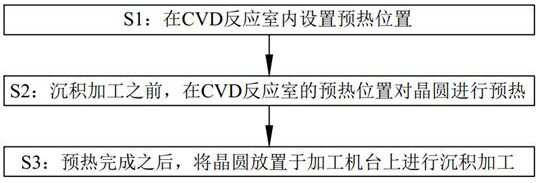
[0030] This embodiment discloses a wafer deposition processing method for CVD equipment.

[0031] Such as figure 1 Shown, be used for the wafer deposition processing method of CVD equipment, comprise the following steps:

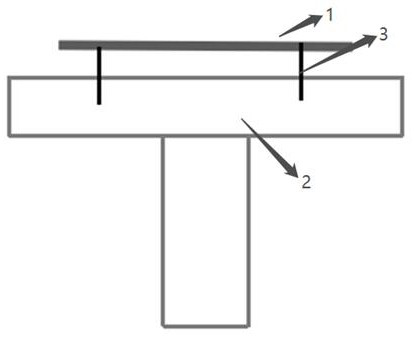
[0032] S1: Set a preheating position in the CVD reaction chamber; the preheating position is set above the processing machine.

[0033] S2: Before the deposition process, preheat the wafer at the preheating position of the CVD reaction chamber (such as figure 2 shown); the wafer is preheated by the gas flow used to process the wafer for deposition.

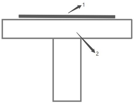
[0034] S3: After the preheating is completed, the wafer is placed on the processing machine for deposition processing (such as image 3 shown).

[0035] The invention preheats the wafer first, so that the wafer can reach a relatively high initial temperature, and then contacts with a high-temperature (400°C) processing machine for deposition processing, thereby solving the problem that the wafer heating cur...


PUM


Abstract

The invention relates to the technical field of CVD equipment processing, and particularly relates to a wafer deposition processing method for CVD equipment. The method comprises the following steps: setting a preheating position in a CVD reaction chamber; before deposition processing, preheating the wafer at the preheating position of the CVD reaction chamber; and after preheating is completed, placing the wafer on a processing machine table for deposition processing. According to the wafer deposition processing method, the wafer breakage rate during wafer CVD deposition processing can be reduced so that the utilization rate of CVD equipment can be improved in an auxiliary manner.

Description

technical field [0001] The invention relates to the technical field of CVD equipment processing, in particular to a wafer deposition processing method for CVD equipment. Background technique [0002] Chemical vapor deposition (Chemical Vapor Deposition, CVD) refers to the reaction of chemical gases or vapors on the surface of the substrate to synthesize coatings or nanomaterials. It is the most widely used technology in the semiconductor industry to deposit a variety of materials, including a wide range of insulating materials. , most metal materials and metal alloy materials. During the deposition process, the gaseous reactant or liquid reactant vapor containing the film elements and other gases required for the reaction are introduced into the CVD reaction chamber, and a chemical reaction occurs on the substrate surface to form a film. The deposition temperature of CVD technology is low, the composition of the film is easy to control, the film thickness is proportional to...

Claims


Application Information

Patent Timeline
Patent Type & Authority Applications(China)
IPC IPC(8): C23C16/46C23C16/458
CPCC23C16/46C23C16/4583
Inventor 王巧罗林邹平刘涵
Owner 重庆忽米网络科技有限公司
Why Eureka
Try Eureka