
Manufacturing method of contact hole for semiconductor device

A manufacturing method and contact hole technology, which are used in semiconductor/solid-state device manufacturing, electrical components, circuits, etc., can solve the problems of insufficient etching amount and over-etching cost in the manufacturing process of contact holes, and achieve lower variability and uniform performance. good effect

Inactive Publication Date: 2022-02-25
MACAU SEMICON CORP LTD +1
View PDF9 Cites 0 Cited by
  • Summary
  • Abstract
  • Description
  • Claims
  • Application Information

AI Technical Summary

Problems solved by technology

[0004] In view of the deficiencies in the background technology, the present invention provides a method for manufacturing a contact hole for a semiconductor device. The technical problem to be solved is that the existing contact hole manufacturing process has the problems of insufficient etching, overetching and high cost.

Method used


Image

  • Manufacturing method of contact hole for semiconductor device
  • Manufacturing method of contact hole for semiconductor device
  • Manufacturing method of contact hole for semiconductor device

Examples


Embodiment Construction

[0026] Illustrative embodiments of the present application include, but are not limited to, a method for fabricating a contact hole of a semiconductor device.

[0027] Reference will now be made in detail to the exemplary embodiments, examples of which are illustrated in the accompanying drawings. When the following description refers to the accompanying drawings, the same numerals in different drawings refer to the same or similar elements unless otherwise indicated. The implementations described in the following exemplary embodiments do not represent all implementations consistent with this application. Rather, they are merely examples of apparatuses and methods consistent with aspects of the present application as recited in the appended claims. The terminology used in this application is for the purpose of describing particular embodiments only, and is not intended to limit the application. As used in this application and the appended claims, the singular forms "a", "the...


PUM


Abstract

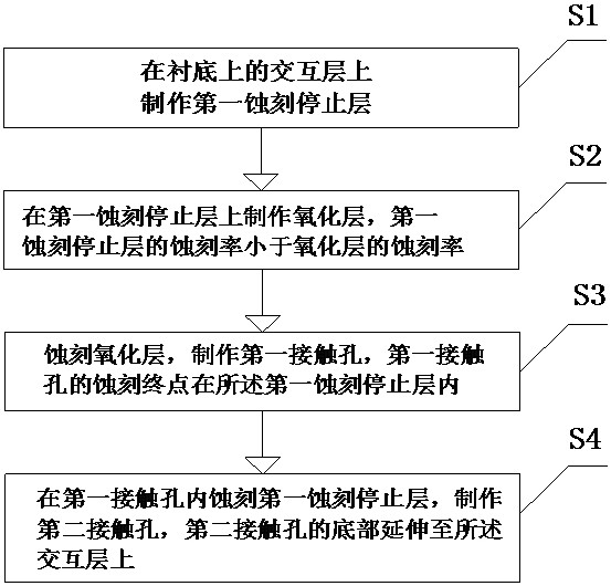
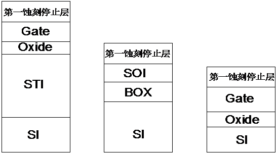
The invention relates to the technical field of semiconductors, and discloses a manufacturing method of a contact hole for a semiconductor device, which comprises the following steps: S1, manufacturing a first etching stop layer on an interaction layer on a substrate; S2, manufacturing an oxide layer on the first etching stop layer, wherein the etching rate of the first etching stop layer is smaller than that of the oxide layer; S3, etching the oxide layer, and manufacturing a first contact hole, wherein the etching end point of the first contact hole is in the first etching stop layer; S4, etching a first etching stop layer in the first contact hole, manufacturing a second contact hole, wherein the bottom of the second contact hole extends to the interaction layer. In actual use, through the first etching stop layer, the etching end points in the step S3 can be located on the first etching stop layer, and then secondary etching is carried out on the first etching stop layer to manufacture the complete contact hole. Therefore, the condition of over-etching or insufficient etching of the contact holes at different positions is avoided, the difference of all the contact holes is reduced, and the performance uniformity is good.

Description

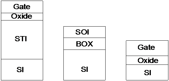
technical field [0001] The invention relates to the technical field of semiconductors, in particular to a method for manufacturing a contact hole of a semiconductor device. Background technique [0002] In the manufacturing process of integrated circuits, the circuit image is transferred to the wafer through processes such as exposure, development and etching. After the circuit diagram is drawn on the wafer, a metal interconnection layer will be made on the wafer. Contact holes are made on the connecting layer and metal electrodes are made on the contact holes to realize the interconnection of electronic devices on the wafer and the interaction between the circuits on the wafer and peripheral signals. [0003] As the integration of integrated circuits on the wafer becomes higher and higher, the number of electronic components on the wafer is also increasing, and correspondingly, the requirements for the manufacturing process of the contact holes are also more stringent. In ...

Claims


Application Information

Patent Timeline
IPC IPC(8): H01L21/768
CPCH01L21/76802H01L21/76805H01L21/76895
Inventor 毛永吉叶甜春朱纪军罗军李彬鸿赵杰
Owner MACAU SEMICON CORP LTD
Learn More