Photovoltaic module and preparation method thereof
A photovoltaic module and transparent ink technology, applied in the field of solar cells, can solve the problems affecting the power generation efficiency and appearance of BIPV modules, the reduction of photoelectric conversion efficiency, and the weakening of the light intensity of cells, so as to overcome pattern distortion, increase surface area, and improve combination The effect of intensity
- Summary
- Abstract
- Description
- Claims
- Application Information
AI Technical Summary
Problems solved by technology
Method used
Image
Examples
preparation example Construction
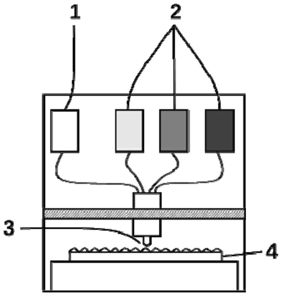
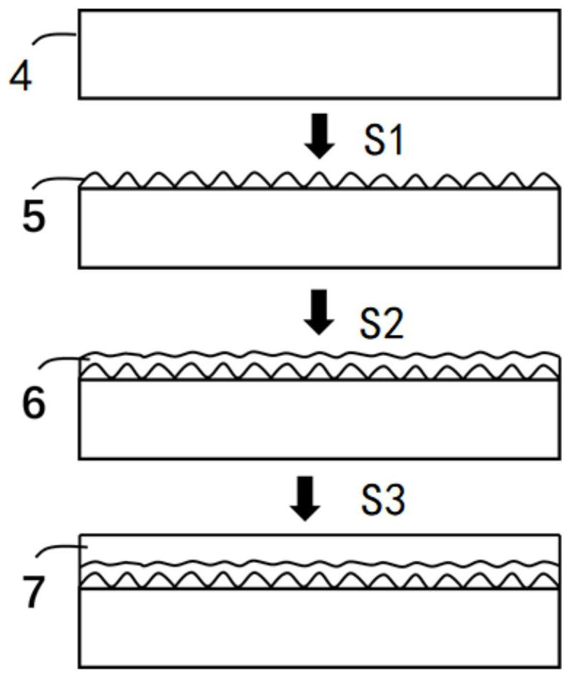
[0034] Figure 1-3 A method for preparing a photovoltaic module according to an embodiment of the present invention is illustrated, including the following steps:
[0035] S1: roughening the surface of the glass substrate 4 to obtain a rough layer 5;
[0036] S2: After cleaning the rough layer 5, print a transparent ink layer 6 on the surface of the rough layer by using UV inkjet transparent ink 1;
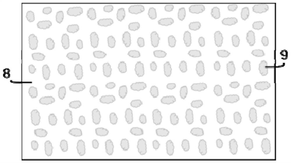
[0037] S3: Print the color ink layer 7 on the surface of the transparent ink layer 6 by using UV inkjet transparent ink 1 and color ink 2, and finally form the transparent ink area 8 and the color ink area 9 on the surface of the component.
[0038]Preferably, before depositing the transparent ink layer 6, a silicon dioxide layer can be sprayed on a clean rough glass surface by UV inkjet, that is, it is arranged between the rough layer 5 and the transparent ink layer 6; Organic solvents and silica particles in the nanometer to micrometer range.
[0039] Preferably, the glass su...
Embodiment 1
[0043] The surface of the ultra-clear glass with a thickness of 5mm is roughened by sandblasting. The surface roughness of the glass is 0.3 microns. The surface of the rough glass is cleaned with a brush and deionized water to remove surface impurities and oil stains, and then through UV Prepare a transparent ink layer with a thickness of about 1.5 microns by inkjet printing, and then prepare a surface with transparent ink accounting for about 70% of the total area by UV inkjet printing, and a color ink layer with red and green inks accounting for 30%. Color ink The thickness of the layer is about 2 microns, and the BIPV module is prepared by encapsulating EVB material and black crystalline silicon cells. The module finally presents a special pattern with red, green and cell colors. After the test of the bonding force of the Baige coating, the coating of this example did not appear to fall off obviously, and the color ink and the glass have a strong bonding strength. The test u...
Embodiment 2
[0045] Use acid etching to roughen the surface of ultra-clear glass with a thickness of 3 mm. The surface roughness of the glass is about 0.05 μm. Use brushes and deionized water to clean the rough glass surface to remove surface impurities and oil stains. The method of inkjet printing evenly sprays a layer of silica sol to increase the bonding strength of glass and ink. After uniform coating, the organic solvent (as a diluent) volatilizes, and finally forms a layer of glass surface with a thickness of 0.2 microns on the glass surface. Silica layer, and then prepare a transparent ink layer with a thickness of about 0.5 microns by UV inkjet printing, and then prepare a surface with transparent ink accounting for about 50% of the total area, and a color ink layer with yellow and orange ink accounting for 50%. The thickness of the ink layer is 2 microns, and the BIPV module is prepared by encapsulating the EVB material and the black crystalline silicon battery. The module finally ...
PUM
| Property | Measurement | Unit |
|---|---|---|
| Thickness | aaaaa | aaaaa |
| Thickness | aaaaa | aaaaa |
| Thickness | aaaaa | aaaaa |
Abstract
Description
Claims
Application Information


