
Assembly for guiding gas circulation in silicon wafer epitaxial process and epitaxial growth device

An epitaxial process and guide technology, which is applied in the field of semiconductor silicon wafer production, can solve the problems of gas loss on the surface of silicon wafers, the inability to realize the thickness of the epitaxial layer, and insufficient guarantee of installation accuracy, so as to avoid overall uneven distribution and avoid Effect of Local Gas Loss, Flatness and Thickness Uniformity Guarantee

Pending Publication Date: 2022-03-01
XIAN ESWIN MATERIAL TECH CO LTD +1
View PDF5 Cites 0 Cited by
  • Summary
  • Abstract
  • Description
  • Claims
  • Application Information

AI Technical Summary

Problems solved by technology

[0005] In order to solve the above technical problems, the embodiment of the present invention expects to provide a component for guiding gas flow in the epitaxial process of silicon wafers and a device for epitaxial growth of silicon wafers, even when the base ring is installed relative to the bushing. The installation accuracy is not guaranteed enough, and multiple guide partitions can also be aligned with corresponding multiple bushing partitions one by one, avoiding the situation where the thickness of the entire epitaxial layer cannot be adjusted, and avoiding the silicon wafer surface. Local gas loss and overall uneven distribution, the flatness and thickness uniformity of epitaxial silicon wafers are guaranteed

Method used


Image

  • Assembly for guiding gas circulation in silicon wafer epitaxial process and epitaxial growth device
  • Assembly for guiding gas circulation in silicon wafer epitaxial process and epitaxial growth device
  • Assembly for guiding gas circulation in silicon wafer epitaxial process and epitaxial growth device

Examples


Embodiment Construction

[0042] The following will clearly and completely describe the technical solutions in the embodiments of the present invention with reference to the drawings in the embodiments of the present invention.

[0043] see Figure 8 , which shows a top view of an assembly 10 for guiding the flow of gas G during the epitaxial process of a silicon wafer W provided by an embodiment of the present invention. Figure 8In , the silicon wafer W is schematically shown by the hatched area filled by the box, and the gas G is schematically shown by the parallel arrow lines. It should also be noted that in this article, there will be no flow to the silicon wafer W or The gas G that has not yet reacted with the silicon wafer W is called the reactive gas RG, and the gas G that has flowed through the silicon wafer W or has reacted with the silicon wafer W is called the reaction tail gas TG. The assembly 10 may include:

[0044] Surrounding the base ring 11 of the silicon wafer W, the base ring 11 h...


PUM


Abstract

The embodiment of the invention discloses an assembly for guiding gas circulation in a silicon wafer epitaxy process and an epitaxial growth device. The assembly comprises a base ring which surrounds a silicon wafer and is provided with a gas inlet embedding hole; the first gas inlet guide piece is embedded in the gas inlet embedding hole, defines a first gas inlet channel used for guiding reaction gas to horizontally flow towards the silicon wafer, and comprises a plurality of first partition plates used for partitioning the first gas inlet channel; the annular lining is arranged between the base ring and the silicon wafer; the top surface of the lining is used for guiding the reaction gas from the first gas inlet guide piece to circulate towards the silicon wafer; the second gas inlet guide piece is arranged between the first gas inlet guide piece and the lining, defines a second gas inlet channel for guiding the reaction gas leaving the first gas inlet guide piece to vertically and upwards flow towards the silicon wafer, and comprises a plurality of second partition plates which are used for separating the second gas inlet channel and correspond to the plurality of first partition plates; the second intake guide is disposed to remain fixed relative to the first intake guide.

Description

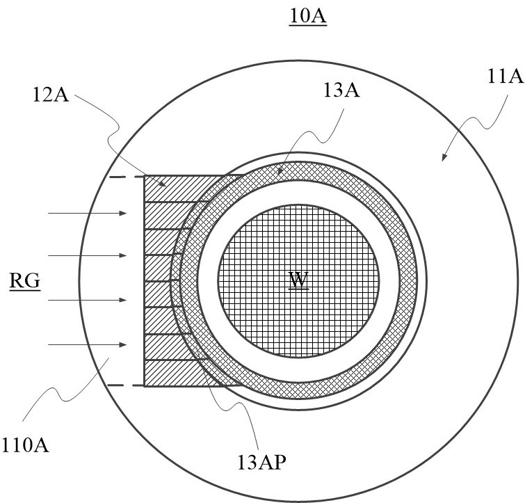
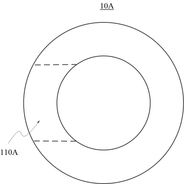
technical field [0001] The invention relates to the field of semiconductor silicon chip production, in particular to a component for guiding gas flow in the silicon chip epitaxial process and a device for the silicon chip epitaxial growth. Background technique [0002] In the production process of epitaxial silicon wafers, the method of chemical vapor deposition is generally used to guide the silicon source gas or reaction gas to the surface of the silicon wafer carried in the process chamber of the high-temperature closed reaction furnace to grow on the upper surface of the silicon wafer. An epitaxial layer. Compared with polished silicon wafers, epitaxial silicon wafers have the advantages of less surface defects and the ability to control the thickness and resistivity of the epitaxial layer. [0003] In the current reactor, see figure 1 Shown in plan view, the assembly 10A for guiding the reaction gas RG schematically shown by parallel arrow lines to the silicon wafer W...

Claims


Application Information

Patent Timeline
Patent Type & Authority Applications(China)
IPC IPC(8): C30B25/14C30B29/06C30B25/12C30B25/08
CPCC30B25/14C23C16/45591C23C16/45559
Inventor 刘凯金柱炫
Owner XIAN ESWIN MATERIAL TECH CO LTD
Learn More