High-precision Mini-LED board electrical testing method

A mini-led, high-precision technology, applied to the parts of electrical measuring instruments, measuring electronics, measuring devices, etc., can solve the problems of high difficulty and high cost, and achieve the effect of reducing density, reducing wear, and reducing the difficulty of testing

Inactive Publication Date: 2022-03-04
GUANGDONG KINGSHINE ELECTRONICS TECH CO LTD
View PDF11 Cites 0 Cited by
  • Summary
  • Abstract
  • Description
  • Claims
  • Application Information

AI Technical Summary

Problems solved by technology

[0002] see figure 1 For high-precision Mini-LED products, since the wafer (4) on the Mini-LED pad (301) is small, the wafer (4) is only 100x200 microns, so the overall Mini-LED product is to ensure that the wafer light does not It will be reflected to the Mini-LED pad (301) and affect the light effect, so the overall area of ​​the two Mini-LED pads (301) is smaller than the size of the wafer (4). Currently, the size of the Mini-LED pad (301) has been made To 60x100 microns, the conventional test pin size is 150 microns, so it is difficult and costly to measure the Mini-LED pads (301) of Mini-LED products, so it is necessary to "a high-precision Mini-LED board electrical measurement method” to solve the above problems

Method used


Image

  • High-precision Mini-LED board electrical testing method
  • High-precision Mini-LED board electrical testing method
  • High-precision Mini-LED board electrical testing method

Examples


Embodiment Construction

[0055] The following will clearly and completely describe the technical solutions in the embodiments of the present invention in conjunction with the accompanying drawings in the embodiments of the present invention, but this does not constitute a limitation to the protection scope of the present invention.

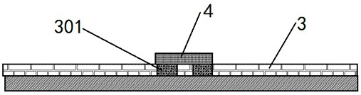
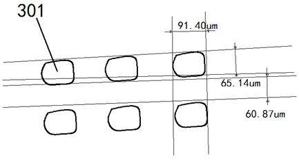
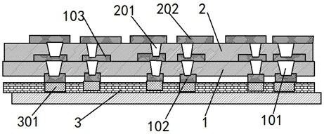
[0056] In the present invention, for a clearer description, the following description is made: the observer faces the attached image 3 For observation, the left side of the observer is set as left, the right side of the observer is set as right, the front of the observer is set as front, the back of the observer is set as back, the top of the observer is set as up, and the bottom of the observer is set as bottom. It should be pointed out in the text The terms "front end", "rear end", "left side", "right side", "middle", "above", "below", etc. indicating the orientation or positional relationship are based on the orientation or positional relationship set in the drawings a...


PUM

PropertyMeasurementUnit
diameteraaaaaaaaaa
diameteraaaaaaaaaa
thicknessaaaaaaaaaa

Abstract

The invention discloses a high-precision Mini-LED board electrical testing method. The high-precision Mini-LED board electrical testing method comprises the following steps: S1.1, switching a board substrate; s1.2, drilling is carried out; s1.3, single-face copper reduction browning is carried out; s1.4, performing laser treatment: performing laser treatment on the upper end surface of the first adapter plate substrate to form at least two first blind holes; s1.5, single-side copper deposition and electroplating: performing copper deposition and electroplating on the upper end surface of the first adapter plate substrate; s1.6, etching bases and bonding pads: etching at least two bases on the lower end face of the first adapter plate substrate; at least two first bonding pads are etched on the upper end face of the first adapter plate substrate, and the base is in bridge connection with the first bonding pads through the first blind holes; s3.1, forming an adapter plate; and S4, electrical testing. According to the method, the step design is reasonable, the size of the bonding pad is enlarged to 300 micrometers from 60 * 100 micrometers through the adapter plate, and measurement of a common flying probe machine is facilitated.

Description

technical field [0001] The invention relates to the technical field of electrical measurement of Mini-LED boards, in particular to a method for electrical measurement of high-precision Mini-LED boards. Background technique [0002] see figure 1 For high-precision Mini-LED products, because the wafer (4) on the Mini-LED pad (301) is small, the wafer (4) is only 100x200 microns, so the overall Mini-LED product is to ensure that the wafer does not light It will be reflected to the Mini-LED pad (301) and affect the light effect, so the overall area of ​​the two Mini-LED pads (301) should be smaller than the size of the wafer (4). At present, the size of the Mini-LED pad (301) has been made To 60x100 microns, the conventional test pin size is 150 microns, so it is difficult and costly to measure the Mini-LED pads (301) of Mini-LED products, so it is necessary to "a high-precision Mini-LED board electrical method” to solve the above problems. [0003] Principle supplement and e...

Claims


Application Information

Patent Timeline
Patent Type & Authority Applications(China)
IPC IPC(8): G01R31/26G01R31/54G01R1/04G01R1/067
CPCG01R31/2601G01R31/54G01R1/0408G01R1/06711
Inventor 颜怡锋陈子濬王欣
Owner GUANGDONG KINGSHINE ELECTRONICS TECH CO LTD
Why Eureka
Try Eureka