Antimony triselenide silicon-based electric dimming switch, optical switch array and chip

A technology of antimony triselenide and optical switch array, which is applied in optics, nonlinear optics, instruments, etc., and can solve the problem of large loss and crosstalk of optical switch chips, high power consumption of optical switch chip drive, and low tuning efficiency of switching units. problems, to achieve the effect of increasing storage density, improving manufacturing and testing compatibility, and reducing energy consumption for device regulation

Inactive Publication Date: 2022-03-04
程唐盛 +1
View PDF3 Cites 2 Cited by
  • Summary
  • Abstract
  • Description
  • Claims
  • Application Information

AI Technical Summary

Problems solved by technology

These schemes can be better compatible with the CMOS process, and can achieve faster switching speeds (nanosecond order) on a relatively small volume (hundreds of microns), but there are also the following deficiencies: 1. The loss of the optical switch chip and large crosstalk
The transmission loss of silicon waveguide is large (usually about 3dB / cm), and the carrier dispersion effect electro-optic tuning has low isolation to light and large crosstalk
2. The drive power consumption of the optical switch chip is high and volatile
Both thermal regulation and electric regulation need to consume a lot of power to maintain a certain switching state, and the switching state cannot be maintained after power off
3. The switching unit has low tuning efficiency and large size
[0004] The current electro-reconfigurable phase-change photonic device technical solutions still have the following problems to be solved urgently: 1. The optical constant contrast of the phase-change materials used in the existing solutions is not large enough in the communication band, and the loss is high; 2. The common disadvantages of phase transition process are relatively large randomness, low accuracy, and poor reconstruction stability; 3. The advantages of plasma electric phase transition are that the energy required for regulation is small, and the size of the device is small, but the static insertion of the optical path Large loss, not suitable for integration; 4. The micro-heater-induced phase change solution has a medium device size and has a certain insertion loss for the optical path

Method used


Image

  • Antimony triselenide silicon-based electric dimming switch, optical switch array and chip
  • Antimony triselenide silicon-based electric dimming switch, optical switch array and chip
  • Antimony triselenide silicon-based electric dimming switch, optical switch array and chip

Examples


Embodiment 1

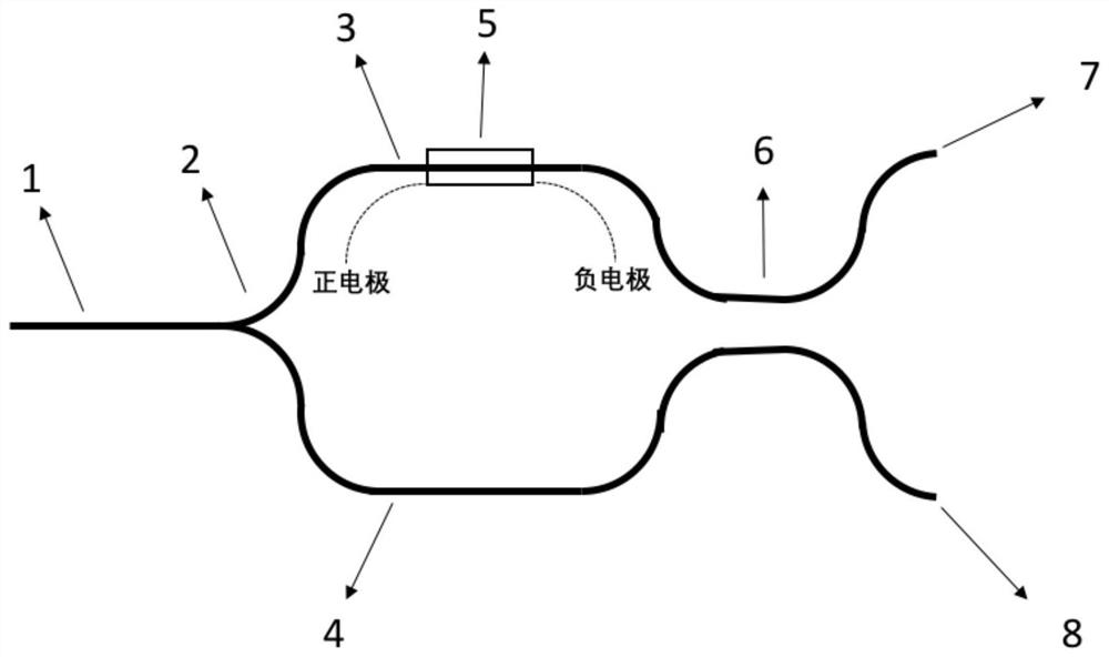
[0035] This embodiment provides the first silicon-based electrical dimming switch based on antimony triselenide, which is realized based on a Mach-Zehnder interferometer (MZI) structure, such as figure 1 As shown, it includes a first input optical waveguide 1, a 1×2 branch optical waveguide 2, an interference arm optical waveguide 3, a reference arm optical waveguide 4, a directional coupler 6, a first output optical waveguide 7 and a second output optical waveguide 8, The output end of the first input optical waveguide 1 is connected to the input end of the 1×2 branch optical waveguide 2, and the two output ends of the 1×2 branch optical waveguide 2 are respectively connected to the interference arm optical waveguide 3 and the reference arm optical waveguide 4 The input end of the interference arm optical waveguide 3 and the output end of the reference arm optical waveguide 4 are respectively connected to the two input ends of the directional coupler 6, and the two output ends...

Embodiment 2

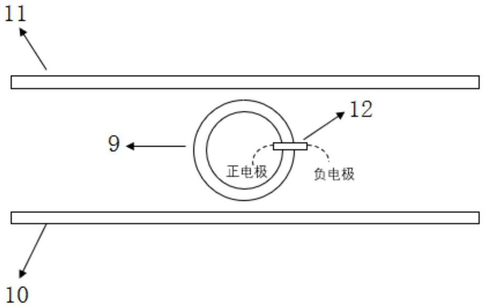
[0045] This embodiment provides a low-power silicon-based phase-change electric dimming switch array, such as Image 6 As shown, the optical switch array is composed of a cascaded series of the first antimony triselenide silicon-based electrical dimming switches in the above-mentioned embodiments. That is, the first output optical waveguide 7 and the second output optical waveguide 8 of the upper-level optical switch are respectively connected to the first input optical waveguide 1 of a lower-level optical switch, and n optical switches are cascaded in this way (1× 2 optical switches) to form an optical switch array. 1XN optical switch array can be used for multi-channel network detection, protection, multi-device testing, industrial automation, and all-optical interactive network construction. The number of output terminals can be set according to the user's needs. Each 1x2 optical switch is a fixed design. For example, if the user needs a 1x4 optical switch, the two output ...

Embodiment 3

[0048] This embodiment provides a low-power silicon-based phase-change electric dimming switch chip, which includes a doped silicon substrate, and any low-power silicon-based phase change chip in the above-mentioned embodiment 2 is integrated on the doped silicon substrate. Transformer dimmer switch array.


PUM


Abstract

The invention relates to the technical field of optical communication devices, in particular to an antimony triselenide silicon-based electric dimming switch, an optical switch array and a chip. Comprising the steps that an antimony triselenide phase change material covers an interference arm optical waveguide based on a Mach-Zehnder interferometer structure to form an antimony triselenide silicon-based electric dimmer switch, and an antimony triselenide phase change material covers a micro-ring optical waveguide based on a micro-ring structure to form the antimony triselenide silicon-based electric dimmer switch. A plurality of two types of antimony triselenide silicon-based electric dimmer switches are respectively cascaded to form two types of antimony triselenide silicon-based electric dimmer switch arrays. By adopting the antimony triselenide phase change material, the energy consumption can be effectively reduced, the device size can be reduced, and the electro-phase change performance can be better on the premise of ensuring small insertion loss.

Description

technical field [0001] The invention relates to the technical field of optical communication devices, in particular to an antimony triselenide silicon-based electric dimming switch, an optical switch array and a chip. Background technique [0002] Most of the traditional optical switch schemes are based on the thermo-optic tuning or electro-optic tuning principle of silicon-based optoelectronics technology, and are realized by Mach-Zehnder interferometer (MZI) structure or micro-ring (MRR) structure. These schemes can be better compatible with the CMOS process, and can achieve faster switching speeds (nanosecond order) on a relatively small volume (hundreds of microns), but there are also the following deficiencies: 1. The loss of the optical switch chip and high crosstalk. The transmission loss of the silicon waveguide is relatively large (usually about 3dB / cm), and the isolation of light is relatively low during the electro-optic tuning of the carrier dispersion effect, a...

Claims


Application Information

Patent Timeline
Patent Type & Authority Applications(China)
IPC IPC(8): G02F1/01G02F1/21
CPCG02F1/011G02F1/0121G02F1/0102G02F1/212
Inventor 程唐盛李璇
Owner 程唐盛
Why Eureka
Try Eureka