Fan-out packaging method and fan-out packaging structure

A packaging method and fan-out technology, applied in electrical components, electric solid-state devices, circuits, etc., can solve the problems of inability to protect and clamp chips, plastic sealing warpage, chip surface cracking, etc., and improve wafer processing. Efficiency, preventing touch and damage, avoiding the effect of flipping and grasping

Pending Publication Date: 2022-03-04
FOREHOPE ELECTRONICS NINGBO CO LTD
View PDF0 Cites 0 Cited by
  • Summary
  • Abstract
  • Description
  • Claims
  • Application Information

AI Technical Summary

Problems solved by technology

[0003] According to the investigation of the inventors, it is found that during the fan-out wafer chip packaging process, there is a problem of warping of the plastic package.
At the same time, fan-out wafer-level chip packaging has strict control over dust fall. Tiny fall dust on the chip can easily lead to ESD breakdown or defects in the package (such as voids, chip surface cracks, etc.), affecting product quality.
In addition, conventional fan-out crystal chips need to perform multiple flipping actions for front or back processing during the production process. In the prior art (chip face up, chip face down), there is only one carrier to prevent chip manufacturing process The warping problem and the protection of the bottom of the chip (convenient for clamping), the chip on the other side cannot be protected and clamped, resulting in many transportation problems

Method used


Image

  • Fan-out packaging method and fan-out packaging structure
  • Fan-out packaging method and fan-out packaging structure
  • Fan-out packaging method and fan-out packaging structure

Examples


no. 1 example

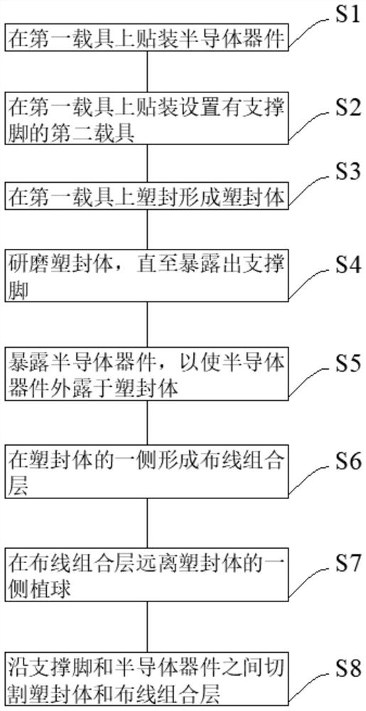
[0078] see figure 1 : This embodiment provides a fan-out packaging method, which is used to prepare a fan-out packaging structure 100, which can solve the problem of warpage of the plastic package in the packaging process, and prevent dust from causing defects, improve product quality, and facilitate Transport and turn over, helping to improve production efficiency.

[0079] The fan-out packaging method provided in this embodiment includes the following steps:

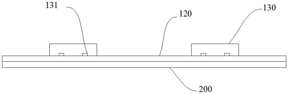
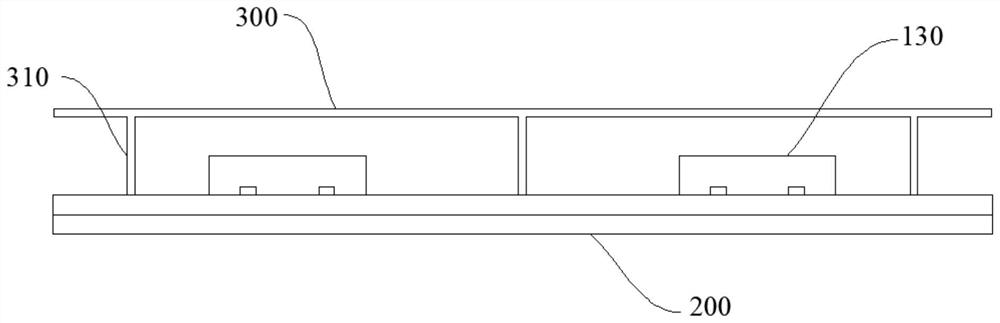
[0080] S1: mounting the semiconductor device 130 on the first carrier 200 .

[0081] see in conjunction figure 2 Specifically, in this embodiment, the fan-out packaging structure 100 is prepared in multiple ways at the same time. Here, firstly, a carrier is provided, on which a plurality of semiconductor devices 130 are simultaneously mounted, and the plurality of semiconductor devices 130 are uniformly arranged in an array, so as to facilitate subsequent cutting to form a plurality of fan-out packaging structures ...

no. 2 example

[0137] This embodiment provides a fan-out packaging method, which is used to prepare the fan-out packaging structure 100, and the basic steps of the method are the same as those of the first embodiment. For details not mentioned in this embodiment, please refer to first embodiment.

[0138] The difference between this embodiment and the first embodiment lies in step S6. In this embodiment, when step S6 is executed, the following steps may be specifically included:

[0139] S61: Form a first dielectric layer 151 on one side of the plastic package 110 .

[0140] Specifically, the first dielectric layer 151 covers the semiconductor device 130 and blocks the conductive pad 131 on the semiconductor device 130 . The first dielectric layer 151 can be formed by spin-coating a dielectric layer, or the first dielectric layer 151 can be prepared by physical vapor deposition (PVD) or chemical vapor deposition (CVD).

[0141] S62: Grooving on the first dielectric layer 151 to form a firs...

no. 3 example

[0154] This embodiment provides a fan-out packaging method for preparing a fan-out packaging structure 100, and the basic steps of the method are the same as those of the first embodiment. For details not mentioned in this embodiment, please refer to Section 1. an embodiment.

[0155] The difference between this embodiment and the first embodiment lies in step S5 and step S6.

[0156] see in conjunction Figure 18 and Figure 19 , in this embodiment, the step of exposing the semiconductor device 130 , that is, when performing step S5 , specifically, grooves may be formed on the first carrier 200 to form a substrate groove 210 penetrating to the semiconductor device 130 .

[0157] Specifically, here, a groove is directly made on the first carrier 200 , so that the semiconductor device 130 is exposed to the plastic package 110 . Specifically, a substrate can be selected here as the first carrier 200, and the base groove 210 is formed by directly grooving on the substrate, and...


PUM


Abstract

The embodiment of the invention provides a fan-out type packaging method and a fan-out type packaging structure, and relates to the technical field of semiconductor packaging, the fan-out type packaging method and the fan-out type packaging structure can provide powerful support in the subsequent plastic packaging process by arranging a second carrier and combining with a first carrier, and the second carrier can reduce backflow impact during plastic packaging, so that the packaging efficiency is improved. Therefore, the plastic package body is prevented from warping. Besides, the second carrier covers the semiconductor device, the lower portion of the semiconductor device is shielded by the first carrier, and the upper portion of the semiconductor device is shielded by the second carrier, so that falling dust in the preparation or transportation process can be shielded, and the problem of ESD breakdown or defects in packaging caused by contact between the falling dust and the internal semiconductor device before plastic packaging is avoided. Moreover, the second carrier can also be used as a clamping object in the transfer process, so that the semiconductor device is prevented from being touched and damaged, front-side grabbing of the wafer is realized, overturning grabbing of the wafer can be avoided, and the wafer processing efficiency is greatly improved.

Description

technical field [0001] The present invention relates to the technical field of semiconductor packaging, in particular to a fan-out packaging method and a fan-out packaging structure. Background technique [0002] With the rapid development of the semiconductor industry, various packaging structures have been fully developed, among which Fan-out wafer level package (FOWLP) technology is widely used in the semiconductor industry. In this packaging technology, a single chip is generally cut from the wafer, and then packaged on a carrier wafer. The main advantages are high-density integration, small size of packaged products, superior product performance, fast signal transmission frequency, etc., fan out technology Mainly to achieve multi-pin output and smaller output pin spacing. [0003] According to the research conducted by the inventors, it is found that during the fan-out wafer chip packaging process, the problem of warping of the plastic package is likely to exist. At t...

Claims


Application Information

Patent Timeline
Patent Type & Authority Applications(China)
IPC IPC(8): H01L23/31H01L21/56H01L23/488H01L21/60
CPCH01L23/3128H01L21/56H01L24/02H01L24/11H01L24/13H01L2224/02331H01L2224/02333H01L2224/02381H01L2224/02379H01L2224/02373H01L2224/111H01L2224/13008
Inventor 徐玉鹏何正鸿
Owner FOREHOPE ELECTRONICS NINGBO CO LTD
Why Eureka
Try Eureka