A kind of semiconductor device and its preparation method

A semiconductor and device technology, applied in the field of semiconductor devices and their preparation, can solve the problems of signal delay, drain efficiency reduction, potential imbalance, etc., and achieve the effects of reducing potential delay, improving drain efficiency, and reducing heat generation

Active Publication Date: 2022-04-12
深圳市时代速信科技有限公司
View PDF7 Cites 0 Cited by
  • Summary
  • Abstract
  • Description
  • Claims
  • Application Information

AI Technical Summary

Problems solved by technology

[0004] The purpose of this application is to provide a semiconductor device and its preparation method in view of the deficiencies in the above-mentioned prior art, so as to solve the problems caused by signal delay and potential imbalance between different grid fingers in the existing fishbone grid structure. The problem of reduced drain efficiency

Method used


Image

  • A kind of semiconductor device and its preparation method
  • A kind of semiconductor device and its preparation method
  • A kind of semiconductor device and its preparation method

Examples


Embodiment Construction

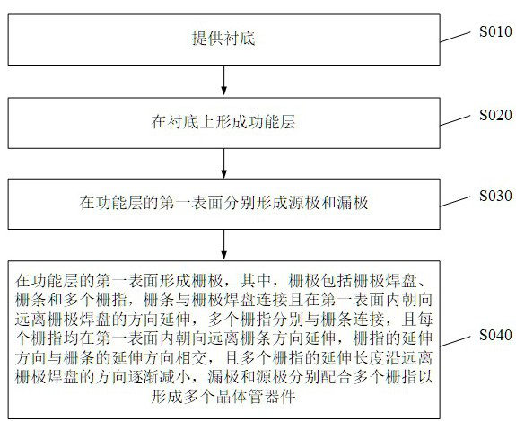
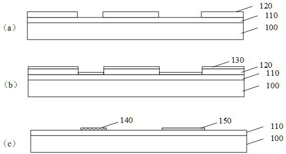
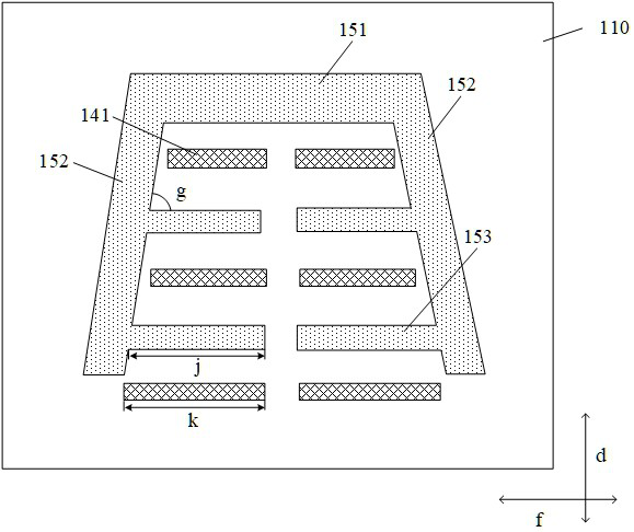
[0031] The embodiments set forth below represent the necessary information to enable those skilled in the art to practice the embodiments, and illustrate the best mode for practicing the embodiments. After reading the following description with reference to the accompanying drawings, those skilled in the art will appreciate the concepts of the present disclosure and will recognize applications of these concepts not specifically set forth herein. It should be understood that these concepts and applications are within the scope of the present disclosure and appended claims.

[0032] It will be understood that, although the terms first, second, etc. may be used herein to describe various elements, these elements should not be limited by these terms. These terms are only used to distinguish one element from another. For example, a first element could be termed a second element, and, similarly, a second element could be termed a first element, without departing from the scope of t...


PUM


Abstract

The present application provides a semiconductor device and its preparation method, which relate to the field of semiconductor technology, including: a substrate and a functional layer on the substrate, and a source, a drain, and a gate are arranged on the first surface of the functional layer; the gate includes A gate pad, a grid bar and a plurality of grid fingers, the grid bar is connected to the gate pad and extends in a direction away from the gate pad in the first surface, the plurality of gate fingers are respectively connected to the grid bar, and each The gate fingers all extend in the direction away from the gate bars in the first surface, and the extension lengths of the multiple gate fingers gradually decrease along the direction away from the gate pad, and the distance between multiple gate fingers can be realized by changing the length of the grid width of a single finger. The potential balance among them improves the drain efficiency and reduces the heat generation. At the same time, the difference in the signal potential transmitted to the farthest end of each gate finger is reduced, and it is basically consistent, thereby reducing the difference between different gate fingers at the farthest end of the gate pad. potential delay.

Description

technical field [0001] The present application relates to the field of semiconductor technology, and in particular, to a semiconductor device and a preparation method thereof. Background technique [0002] Gallium nitride has high breakdown electric field and high electron saturation drift speed of wide bandgap semiconductor material. At the same time, because of the very strong spontaneous and piezoelectric polarization effect of AlGaN / GaN, deep triangular quantum wells can be formed at the hetero interface, and Sensing up to 10 13 cm -2 The magnitude of 2-dimensional electron gas (2DEG) makes it have great advantages compared with other compound semiconductors such as GaAs, InP, etc. in high-power RF electronic devices. For RF power devices led by gallium nitride, when the use frequency increases, the resistance and inductance of the gate are regarded as important factors that determine the gain of the device. [0003] In order to reduce the gate resistance and inductan...

Claims


Application Information

Patent Timeline
Patent Type & Authority Patents(China)
IPC IPC(8): H01L29/423H01L29/778H01L21/335H01L21/28
CPCH01L29/778H01L29/66462H01L29/401H01L29/42316
Inventor 田宇
Owner 深圳市时代速信科技有限公司
Why Eureka
Try Eureka