Semiconductor device

A technology for semiconductors and devices, applied in the field of semiconductor devices, can solve the problems of increasing device area, difficult to meet the requirements of miniaturization and integration of devices, etc., and achieve the effects of improving device quality, reducing parasitic capacitance Cds, and improving drain efficiency

Active Publication Date: 2021-12-14
深圳市时代速信科技有限公司
View PDF0 Cites 0 Cited by
  • Summary
  • Abstract
  • Description
  • Claims
  • Application Information

AI Technical Summary

Problems solved by technology

However, this method of reducing the parasitic capacitance of the source and drain will lead to an increase in the device area, which is difficult to meet the requirements of device miniaturization and integration

Method used


Image

  • Semiconductor device
  • Semiconductor device
  • Semiconductor device

Examples


Embodiment Construction

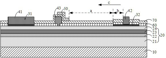
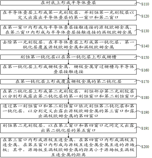
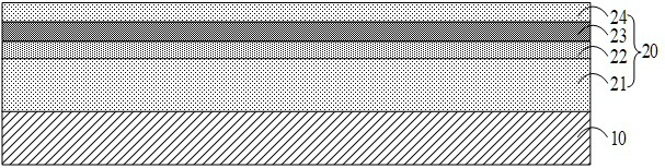
[0048] The embodiments set forth below represent the information necessary to enable one skilled in the art to practice the embodiments and illustrate the best mode of practicing the embodiments. Upon reading the following description with reference to the accompanying drawing figures, those skilled in the art will understand the concepts of the disclosure and will recognize applications of these concepts not specifically addressed herein. It should be understood that these concepts and applications are within the scope of this disclosure and the appended claims.

[0049] It will be understood that, although the terms first, second, etc. may be used herein to describe various elements, these elements should not be limited by these terms. These terms are only used to distinguish one element from another. For example, a first element could be termed a second element, and, similarly, a second element could be termed a first element, without departing from the scope of the presen...


PUM


Abstract

A semiconductor device relates to the technical field of semiconductors. The semiconductor device includes a substrate, a semiconductor stack on the substrate, a source ohmic metal and a drain ohmic metal arranged at intervals on the semiconductor stack, a source interconnection metal connected to the source ohmic metal, The drain interconnect metal is in contact with the drain ohmic metal, the gate metal is located between the source interconnect metal and the drain interconnect metal and is in contact with the semiconductor stack, and is located on the semiconductor stack and connected to the source The interconnection metal forms the source field plate of the metal interconnection; wherein, the source field plate is located between the source interconnection metal and the drain interconnection metal, and the distance from the source field plate to the drain ohmic metal is smaller than that from the source field plate to the drain interconnection Even the metal distance. The semiconductor device can reduce the parasitic capacitance between the source and the drain without additionally increasing the area of ​​the device, thereby improving the drain efficiency of the device.

Description

technical field [0001] The present disclosure relates to the technical field of semiconductors, and in particular, to a semiconductor device. Background technique [0002] In recent years, the third-generation semiconductors represented by gallium nitride (GaN) have developed rapidly, and better epitaxial structures can be obtained on silicon carbide (SiC), sapphire and silicon substrates. GaN material has a large forbidden band width and high saturation electron drift velocity, which has significant advantages in microwave, especially millimeter wave applications. In addition, GaN materials have high thermal conductivity, high breakdown voltage, strong radiation resistance and good high temperature resistance. They are suitable for making high-frequency, high-efficiency, and high-voltage RF microwave devices. Military radar and 5G communication have also been widely used. [0003] For RF GaN devices, the drain efficiency (Drain efficiency) is one of the key indicators to ...

Claims


Application Information

Patent Timeline
Patent Type & Authority Patents(China)
IPC IPC(8): H01L29/40H01L29/778H01L21/335
CPCH01L29/402H01L29/7786H01L29/66462
Inventor 林坤杨天应刘丽娟吴文垚
Owner 深圳市时代速信科技有限公司
Why Eureka
Try Eureka