Laser tin spraying welding method for welding spots in narrow deep cavity

A tin welding and solder joint technology, applied in the field of laser tin spray welding, can solve the problems of difficult operation, poor consistency, low yield of solder joints, etc., achieve good electrical performance consistency, optimize the process path, and realize the effect of automatic welding

Pending Publication Date: 2022-03-08
CHINA ELECTRONIC TECH GRP CORP NO 38 RES INST
View PDF8 Cites 4 Cited by
  • Summary
  • Abstract
  • Description
  • Claims
  • Application Information

AI Technical Summary

Problems solved by technology

[0005] The purpose of the present invention is to solve the problems of difficult operation, low solder joint yield and poor consistency of the existing welding methods of radio frequency connectors and microstrip circuits, and provides a laser spray tin welding method for solder joints in narrow and deep cavities

Method used


Image

  • Laser tin spraying welding method for welding spots in narrow deep cavity
  • Laser tin spraying welding method for welding spots in narrow deep cavity
  • Laser tin spraying welding method for welding spots in narrow deep cavity

Examples


Embodiment 1

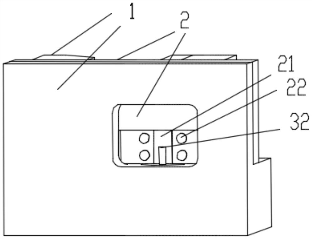
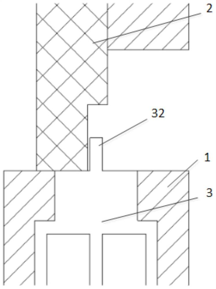
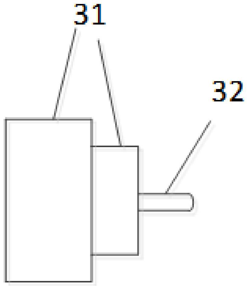
[0041] Such as Figure 1~2 Shown is the welding structure diagram of this embodiment. The gold workpiece 1 is an aluminum-silicon alloy, the microstrip board 2 is a multilayer structure and the welding area is slotted, and the radio frequency connector 3 includes an outer conductor 31 and an inner conductor 32 ( image 3 ), the microstrip board 2 and the outer conductor 31 of the radio frequency connector are welded on the gold workpiece 1, and the inner conductor 32 of the radio frequency connector is lapped on the pad 21 of the microstrip board 2, and the electrical interconnection is realized by laser spray tin welding process. An isolation hole 22 is designed at 0.28 mm on both sides of the pad 21 of the microstrip board, and a short circuit is not allowed during soldering. The surface of the radio frequency connector 3 and the pads of the multilayer microstrip board 2 are gold-plated.

[0042] The cavity 11 of the gold workpiece has a size of 5mm×4.5mm×2.35mm, the width...

Embodiment 2

[0054] Same as Example 1, such as Figure 1~2 Shown is the welding structure diagram of this embodiment.

[0055] In step (1), the diameter of the solder ball is selected to be 0.89mm, and the material of the solder ball is Sn96.5Ag3Cu0.5.

[0056] Steps (2), (3), (4) are the same as in Example 1.

[0057] Step (5) The solder ball slides from the ball supply system to the position of the nozzle, the laser heats the solder ball, and the solder melts and sprays to form a solder joint. The laser energy output is 45%, the time is 70ms, and the spot diameter is 1.1mm.

[0058] In step (6) chasing the light, the energy output of the first light chasing laser is 20%, the time is 620ms, and the diameter of the spot is 1.5mm; the energy output of the second chasing laser is 16%, the time is 750ms, and the diameter of the spot is 1.5mm.

[0059] Step (7) Use water cleaning equipment to clean the solder joints.

[0060] The laser welding process is carried out in a nitrogen atmospher...

Embodiment 3

[0063] Such as Figure 6~7 Shown is the welding structure diagram of embodiment 3. The gold workpiece 1 is an aluminum-silicon alloy, the microstrip board 2 has a multi-layer structure and the welding area is slotted, the radio frequency connector 3 includes an outer conductor 31 and an inner conductor 32, and the microstrip board 2, the microstrip board 2 and the outer conductor of the radio frequency connector 31 are all welded on the gold workpiece 1, and the inner conductor 32 of the radio frequency connector is lapped on the pad 21 of the microstrip board 2, and the electrical interconnection is realized by laser spray tin welding process. An isolation hole 22 is designed at 0.28 mm on both sides of the pad 21 of the microstrip board, and a short circuit is not allowed during soldering. The surface of the radio frequency connector 3 and the pads of the multilayer microstrip board 2 are gold-plated.

[0064] The distance between the boss 12 of the gold workpiece and the ...


PUM

PropertyMeasurementUnit
diameteraaaaaaaaaa
diameteraaaaaaaaaa
diameteraaaaaaaaaa

Abstract

The invention relates to the technical field of electronic assembly, in particular to a laser tin-spraying welding method for a welding spot in a narrow deep cavity, which comprises the following steps of: (1) selecting a tin ball with a proper size; (2) cleaning a position to be welded; (3) coating a soldering flux; (4) laser preheating; (5) discharging balls; (6) light following; according to the laser tin spraying welding method, the welding spots meeting the welding quality and performance indexes are obtained by selecting tin balls with proper sizes, optimizing the process path and reasonably setting process parameters, non-contact, local heating, accurate positioning and efficient welding are achieved, and the problems that manual welding cannot be operated or the operation space is limited, the welding spot qualification rate is low, and the welding quality is poor are solved. And the consistency is poor.

Description

technical field [0001] The invention relates to the technical field of electronic assembly, in particular to a laser spray tin welding method for solder spots in a narrow and deep cavity. Background technique [0002] Phased array radar is a kind of radar system widely used at present. With the development of system design toward miniaturization, complex structure, and functional integration, extremely high requirements are placed on the volume and weight of the radar. As the core component of phased array radar, the antenna unit uses a large number of radio frequency connectors to realize electrical interconnection in order to improve system integration. This is because the RF connector has the advantages of small size, light weight, superior RF performance, and low loss. [0003] The interconnection between the RF connector and the microstrip circuit is generally achieved by manual soldering, but for narrow and deep cavity structures, manual soldering cannot be performed...

Claims


Application Information

Patent Timeline
Patent Type & Authority Applications(China)
IPC IPC(8): B23K3/00B23K3/08B23K101/36
CPCB23K3/00B23K3/08B23K2101/36
Inventor 李苗杨兆军宋惠东李森周自泉邹嘉佳程明生洪肇斌
Owner CHINA ELECTRONIC TECH GRP CORP NO 38 RES INST
Why Eureka
Try Eureka