
Eureka
For R&D, Eureka makes reading and utilizing patents & technical documents easy.
Eureka AIR
Designed for self-driven R&D workflows. Generate viable solutions, solve complex R&D challenges, empower your innovation with AI.

Eureka Materials
Designed for material experts only. Revolutionize your material R&D, from search, analyze, to developing new materials.

TechResearch
Generate reliable direction feasibility study reports for your R&D in just a few steps.

TechSeek
Discover and master advanced knowledge NOW. Basics, ideas, possibilities, all at once.

TechMind
As an expert in R&D Theories, TechMind can generates customized viable solutions instantly.

TechRisk
Analyze your overall solution with one click, know your potential R&D risks in advance.

TechMonitor
Get weekly tech updates, stay abreast of the latest tech innovations and key insights.
Photolithographic glass and microstructure processing method thereof
A microstructure and photolithography technology, applied in glass furnace equipment, glass manufacturing equipment, manufacturing tools, etc., can solve problems such as misalignment
- Summary
- Abstract
- Description
- Claims
- Application Information
AI Technical Summary
Problems solved by technology
Method used
Image

Examples
Embodiment 1-8
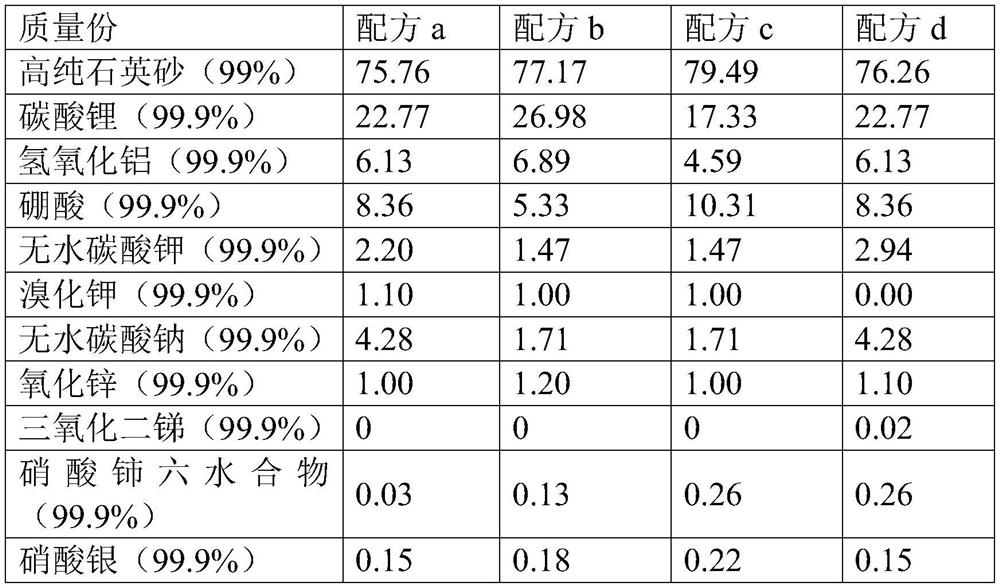
[0056] Examples 1-8 are examples of photolithographic glass of the present invention, wherein Examples 1-4 respectively adopt the glass raw material formulas a-d shown in Table 1, and are prepared by the following preparation method 1, and the prepared glasses have the following properties: Components a-d shown in Table 2; Examples 5-8 were prepared using the glass raw material formulas a-d shown in Table 1, respectively, using the following preparation method 2.
[0057] Table 1 shows the raw material formulations of the photoresistable glasses described in Examples 1-8 of the present invention.
[0058] Table 2 shows the composition of the photoresistable glasses described in Examples 1-4 of the present invention.
[0059] The raw material formula of the photoetching glass of table 1 embodiment 1-8
[0060]
[0061] The composition of the photoetching glass of table 2 embodiment 1-4
[0062] parts by mass Component a Component b component c component d...
Embodiment 9
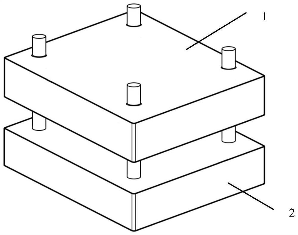
[0082] This embodiment provides a photolithography method for photolithographic glass wafers, which can realize high-quality processing of glass surfaces. The steps are as follows:
[0083] (1) The lithographic glass of Example 2 is optically processed to obtain a plurality of glass wafers with diameters of 2, 3, and 4 inches respectively, and the glass wafers of each diameter are respectively processed to have 200 μm, 300 μm, Multiple glass wafers with thickness of 400μm and 500μm;
[0084] (2) Use a quartz reticle with an aperture of 50 μm and a spacing of 100 μm to expose each glass wafer to ultraviolet light at an exposure wavelength of 316 nm and an energy density of 3.5 W / cm 2 , for the glass wafer exposure, the relationship between the exposure time and the thickness of the glass wafer is as follows: a glass wafer with a thickness of 200 μm was exposed for 15 minutes, a glass wafer with a thickness of 300 μm was exposed for 20 minutes, a glass wafer with a thickness of ...
PUM
 Abstract
Description
Claims
Application Information
 - R&D Engineer
- R&D Manager
- IP Professional
- Industry Leading Data Capabilities
- Powerful AI technology
- Patent DNA Extraction
Browse by: Latest US Patents, China's latest patents, Technical Efficacy Thesaurus, Application Domain, Technology Topic, Popular Technical Reports.
© 2024 PatSnap. All rights reserved.Legal|Privacy policy|Modern Slavery Act Transparency Statement|Sitemap|About US| Contact US: help@patsnap.com