

Film probe card and probe head thereof
A probe card and probe head technology, which is applied in the direction of measuring devices, instruments, and measuring electronics, can solve problems such as unevenness and easy damage of the film, and achieve the effect of preventing excessive contact force and stable and reliable electrical contact
- Summary
- Abstract
- Description
- Claims
- Application Information
AI Technical Summary
Problems solved by technology
Method used
Image

Examples
Embodiment 1
[0048] Embodiment one: see attached Figure 1-6 Shown:
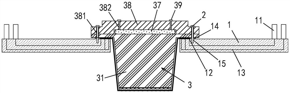
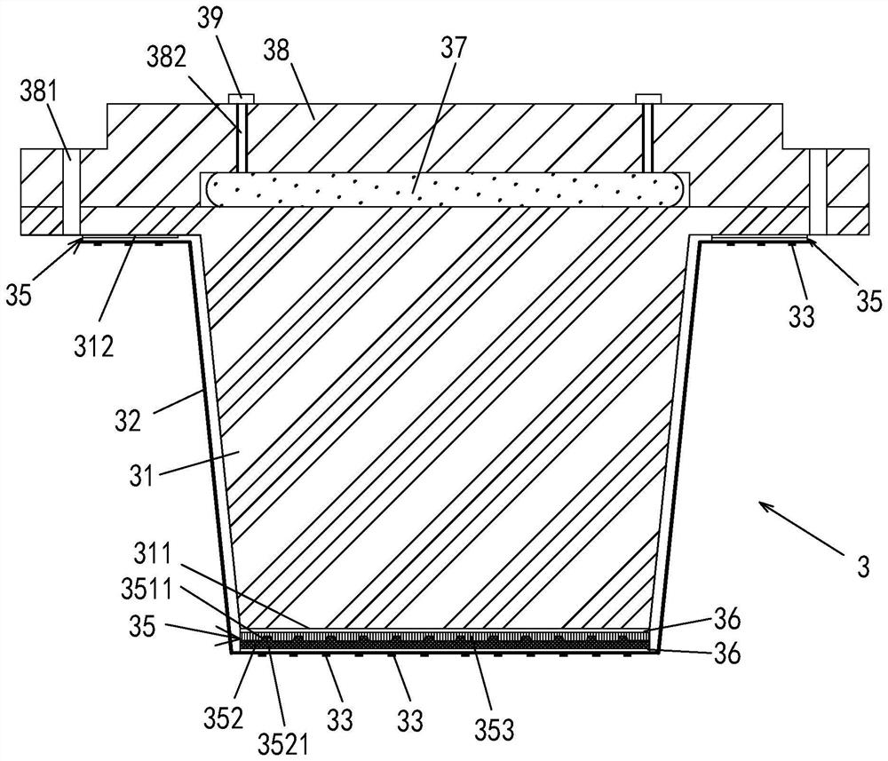
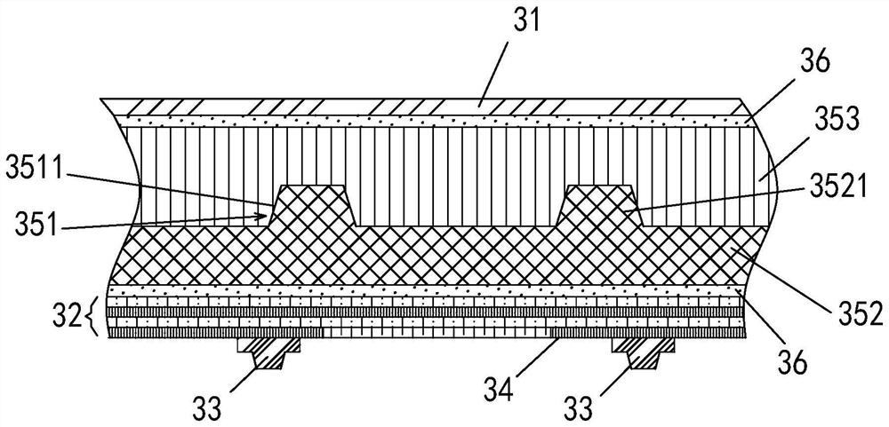
[0049] A thin-film probe card, comprising a PCB board 1, a connector 2, and a thin-film probe head 3; The thin film 32 , and the probes 33 and interconnection lines 34 arranged on the thin film 32 .
[0050] PCB board 1 is a multi-layer epoxy resin circuit board, on which coaxial connectors 11 and signal connection points 12 are distributed, and PCB traces 13 are distributed inside, respectively connecting coaxial connectors 11 to corresponding signal connection points 12, Realize electrical signal conduction and transmission; the surface of PCB 1 is also distributed with spring structures 14 and PCB end threaded holes 15; the center of PCB 1 is hollowed out to accommodate the film probe head 3; spring structure 14 is located in the center of PCB 1 The outer periphery of the hollowed out part is used to realize the tight connection with the film probe head 3 .
[0051] The supporting body 31 is a rigid body with a con...
Embodiment 2
[0062] Embodiment two: see attached Figure 1-6 Shown:
[0063] A film probe head, including a support body 31 providing an action surface 311, a film 32 covering the action surface 311 of the support body 31, and probes 33 and interconnection wires 34 arranged on the film 32, specifically The structure is the same as that of the thin-film probe head in Embodiment 1, and will not be repeated here.
Embodiment 3
[0064] Embodiment three: see attached figure 1 , attached figure 2 , attached Figure 7 and attached Figure 8 Shown:
[0065] A thin-film probe card, comprising a PCB board 1, a connector 2, and a thin-film probe head 3; The thin film 32 , and the probes 33 and interconnection lines 34 arranged on the thin film 32 .
[0066] The difference from Embodiment 1 is that the probes 33 are in a straight line, and the depression 3511 is not a groove, but half of the supporting rigid body 353 is concave upward, that is, the supporting rigid body 353 is half thick and half thin. The thinner side forms the recess 3511, such as Figure 7 , and a column of probes 33 is correspondingly arranged across the wall of the recess 3511, such as Figure 8 shown. The shape of the supporting elastic layer 352 is matched with the lower surface of the supporting rigid body 353, so that the parts on both sides of the probe 33 on the supporting elastic layer 352 have a thickness difference, so t...
PUM
 Abstract
Description
Claims
Application Information