Upper electrode assembly and semiconductor process equipment

A technology of electrode components and process equipment, applied in semiconductor/solid-state device manufacturing, electrical components, circuits, etc., can solve problems such as poor contact electrode temperature control ability, achieve low temperature control difficulty, improve temperature control effect, and increase temperature upper limit Effect

Pending Publication Date: 2022-03-18
BEIJING NAURA MICROELECTRONICS EQUIP CO LTD
View PDF6 Cites 2 Cited by
  • Summary
  • Abstract
  • Description
  • Claims
  • Application Information

AI Technical Summary

Problems solved by technology

[0003] The application discloses an upper electrode assembly and semiconductor process equipment, which can solve the problem of poor temperature control ability of the current contact electrodes

Method used


Image

  • Upper electrode assembly and semiconductor process equipment
  • Upper electrode assembly and semiconductor process equipment
  • Upper electrode assembly and semiconductor process equipment

Examples


Embodiment Construction

[0030] In order to make the purpose, technical solution and advantages of the present application clearer, the technical solution of the present application will be clearly and completely described below in conjunction with specific embodiments of the present application and corresponding drawings. Apparently, the described embodiments are only some of the embodiments of the present application, rather than all the embodiments. Based on the embodiments in this application, all other embodiments obtained by persons of ordinary skill in the art without making creative efforts belong to the scope of protection of this application.

[0031] The technical solutions disclosed in various embodiments of the present application will be described in detail below with reference to the accompanying drawings.

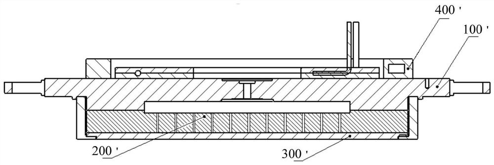
[0032] Such as figure 1 As shown, an upper electrode assembly, in which the heating ring 400' for heating the contact electrode 300' is directly installed on the upper electrode co...


PUM


Abstract

The invention discloses an upper electrode assembly and semiconductor process equipment, the upper electrode assembly comprises an upper electrode cover plate, and the upper electrode cover plate is used for being arranged on a top opening of a reaction chamber; the flow uniformizing piece is a heat conduction structural piece and is installed on the upper electrode cover plate, at least one part of the flow uniformizing piece is located on the side, facing the reaction cavity, of the upper electrode cover plate, and the flow uniformizing piece is provided with an annular containing groove; the contact electrode is arranged on the surface of the side, away from the upper electrode cover plate, of the flow uniformizing piece, and an opening of the annular containing groove is arranged away from the contact electrode; and the heating ring is arranged in the annular accommodating groove. According to the technical scheme, the problems that the heated effect of an existing contact electrode is poor, and the temperature of the upper electrode cover plate is high can be solved.

Description

technical field [0001] The application belongs to the technical field of semiconductor processing, and in particular relates to an upper electrode assembly and semiconductor process equipment. Background technique [0002] With the gradual expansion of the application range of integrated circuits, the etching requirements for integrated circuits are getting higher and higher, and the requirements for etching equipment are also getting higher and higher. Among them, inductively coupled plasma equipment and capacitively coupled plasma equipment in dry etching are most widely used in etching equipment. In both types of etching equipment, the wafer is adsorbed on the electrostatic chuck and located below the equipment, and the process gas is generally supplied from the corresponding structure in the upper electrode assembly above the electrostatic chuck. In the process of wafer processing, in order to obtain a better process effect, it is usually necessary to control the temper...

Claims


Application Information

Patent Timeline
Patent Type & Authority Applications(China)
IPC IPC(8): H01J37/32H01L21/67
CPCH01J37/32568H01J37/32431H01L21/67103H01L21/67213H01L21/67069
Inventor 王家祥邓雅天李凯张鹏
Owner BEIJING NAURA MICROELECTRONICS EQUIP CO LTD
Why Eureka
Try Eureka