Pin-free and welding-free SMD (Surface Mount Device) electronic component

A kind of technology of electronic components and patch type, which is applied in the direction of adding resistors, electrical components, electrical components, etc. at the lead-out end, which can solve the problems of poor anti-combination wave capability, small flow rate, and complicated production, so as to improve the current flow rate , Increase the effective area and reduce the cost

Pending Publication Date: 2022-03-22
贵州凯里经济开发区中昊电子有限公司 +1
View PDF2 Cites 0 Cited by
  • Summary
  • Abstract
  • Description
  • Claims
  • Application Information

AI Technical Summary

Problems solved by technology

[0007] In order to solve the above-mentioned technical problems, the present invention provides a chip-type electronic component without pins and soldering, so as to solve the problem of small current flow, poor anti-combination wave ability, and pressure difference of current chip-type electronic components. High cost, complex production issues

Method used


Image

  • Pin-free and welding-free SMD (Surface Mount Device) electronic component
  • Pin-free and welding-free SMD (Surface Mount Device) electronic component
  • Pin-free and welding-free SMD (Surface Mount Device) electronic component

Examples


Embodiment 1

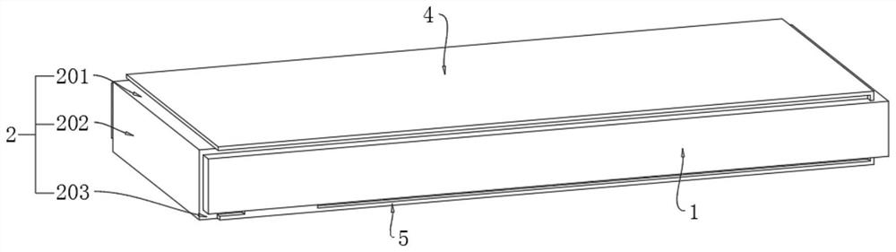
[0029] as attached figure 1 to attach image 3 Shown:

[0030] The present invention provides a chip-type electronic component without pins and soldering, comprising a substrate 1; an upper electrode surface 2 is arranged on the top of the substrate 1; the upper electrode surface 2 consists of an upper electrode layer 201, an auxiliary electrode layer 202 and The upper bonding electrode 203 is composed; the bottom of the substrate 1 is provided with a lower electrode surface 3; the lower electrode surface 3 is composed of a lower electrode layer 301 and a lower bonding electrode 302; the top of the upper electrode surface 2 is covered with an upper insulating layer 4; The bottom of the lower electrode surface 3 is covered with a lower insulating layer 5 ; an isolation gap 6 is provided between the upper bonding electrode 203 and the lower electrode layer 301 .

[0031] Wherein, the substrate 1 is a piezoresistor, and the upper electrode surface 201 , the upper bonding electr...

Embodiment 2

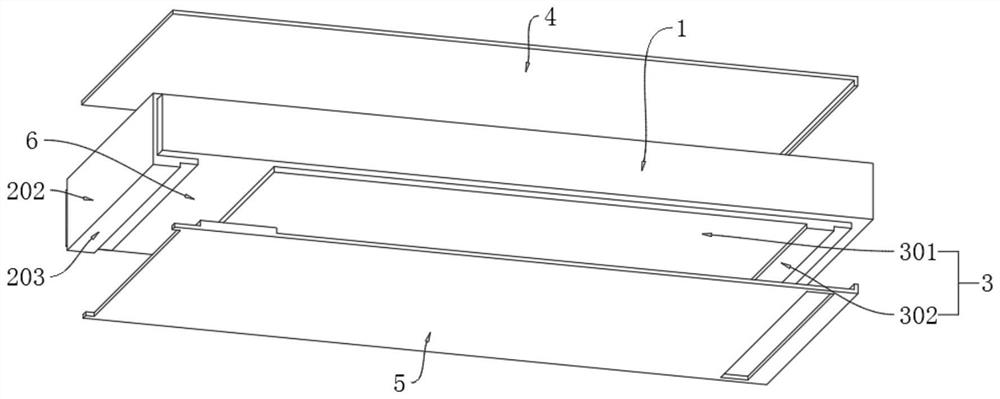
[0040] as attached Figure 4 to attach Figure 5 Shown:

[0041] The present invention provides a chip-type electronic component without pins and soldering, comprising a substrate 1; an upper electrode surface 2 is arranged on the top of the substrate 1; the upper electrode surface 2 consists of an upper electrode layer 201, an auxiliary electrode layer 202 and The upper bonding electrode 203 is composed; the bottom of the substrate 1 is provided with a lower electrode surface 3; the lower electrode surface 3 is composed of a lower electrode layer 301 and a lower bonding electrode 302; the top of the upper electrode surface 2 is covered with an upper insulating layer 4; The bottom of the lower electrode surface 3 is covered with a lower insulating layer 5 ; an isolation gap 6 is provided between the upper bonding electrode 203 and the lower electrode layer 301 .

[0042] Wherein, the substrate 1 is a positive temperature coefficient thermistor, and the upper electrode surfac...

Embodiment 3

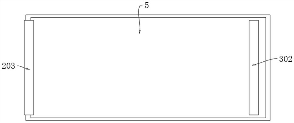
[0050] as attached Image 6 Shown:

[0051] The present invention provides a chip-type electronic component without pins and soldering, comprising a substrate 1; an upper electrode surface 2 is arranged on the top of the substrate 1; the upper electrode surface 2 consists of an upper electrode layer 201, an auxiliary electrode layer 202 and The upper bonding electrode 203 is composed; the bottom of the substrate 1 is provided with a lower electrode surface 3; the lower electrode surface 3 is composed of a lower electrode layer 301 and a lower bonding electrode 302; the top of the upper electrode surface 2 is covered with an upper insulating layer 4; The bottom of the lower electrode surface 3 is covered with a lower insulating layer 5 ; an isolation gap 6 is provided between the upper bonding electrode 203 and the lower electrode layer 301 .

[0052] Wherein, the substrate 1 is a piezoresistor, and the upper electrode surfaces 201, 203 and the lower electrode surface 3 are el...


PUM


Abstract

The invention provides a pin-free and welding-free surface-mounted electronic component, relates to the technical field of electronic components, and solves the problems of small current flow, poor combined wave resistance, poor voltage resistance, high cost and complex production of the existing surface-mounted electronic component. The pin-free and welding-free surface-mounted electronic component comprises a substrate; the upper electrode face is composed of an upper electrode layer, an auxiliary electrode layer and an upper attaching electrode. A lower electrode surface is arranged at the bottom of the base body; the lower electrode face is composed of a lower electrode layer and a lower attaching electrode. The top of the upper electrode surface is covered with an upper insulating layer; the bottom of the lower electrode surface is covered with a lower insulating layer; and an isolation gap is arranged between the upper bonding electrode and the lower electrode layer. According to the device, the effective area of the electrode can be increased, the current flow can be improved, the combined wave resistance can be improved, the lead-free or pin-free and welding-free process technology is adopted, the production environment meets the environment-friendly requirement, the production process is simpler, and the cost can be obviously reduced.

Description

technical field [0001] The invention belongs to the technical field of electronic components, and more specifically relates to a chip-type electronic component without leads and without soldering. Background technique [0002] At present, there are four production methods for SMD electronic components: welding and encapsulating double-legged SMD, single-legged circular SMD, plastic-encapsulated SMD electronic components and multi-layer SMD electronic components, among which welding and encapsulating double-legged SMD The product is encapsulated by traditional welding, the feet are stepped, and can be produced with traditional equipment and technology; the single-leg circular patch is equipped with electrodes on both sides of the substrate, insulating materials are placed on the edges of the electrodes on both sides, and the upper electrode is welded with a flat lead. The foot bracket, the lower electrode and the pin form two bonding surfaces; the plastic-encapsulated SMD ele...

Claims


Application Information

Patent Timeline
Patent Type & Authority Applications(China)
IPC IPC(8): H01C1/14H01C7/102H01C17/28H01G4/005H01G4/228H05K13/04
CPCH01C1/14H01C7/102H01C17/28H01G4/005H01G4/228H05K13/0465
Inventor 朱同江吴燕青胡安苹余熙北石锦均
Owner 贵州凯里经济开发区中昊电子有限公司
Why Eureka
Try Eureka