Power semiconductor device

A technology for power semiconductors and devices, applied in the field of power semiconductor devices, can solve problems such as poor turn-off uniformity of chips, and achieve the effects of improving cathode area utilization, reducing process difficulty, and improving turn-off capability.

Pending Publication Date: 2022-03-22
ZHUZHOU CRRC TIMES SEMICON CO LTD
View PDF0 Cites 0 Cited by
  • Summary
  • Abstract
  • Description
  • Claims
  • Application Information

AI Technical Summary

Problems solved by technology

[0004] In view of the above problems, the present application provides a power semiconductor device, which solves the technical problem of poor turn-off uniformity of the chip caused by the arrangement of the cathode combs of the gate commutated thyristor power semiconductor device in the prior art

Method used


Image

  • Power semiconductor device
  • Power semiconductor device
  • Power semiconductor device

Examples


Embodiment 1

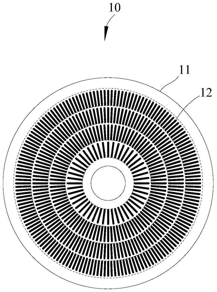
[0062] An embodiment of the present application provides a power semiconductor device 40 , including a wafer 41 and a plurality of first cathode combs 42 and gates 45 disposed on the surface of the wafer 41 .

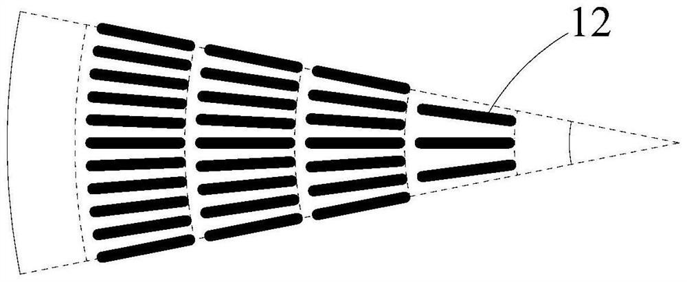
[0063] Among them, such as Figure 4 As shown, the surface of the wafer 41 is divided into a plurality of concentric ring regions 411 and a plurality of concentric sector regions 412 with the same center O, and a plurality of concentric ring regions 411 and a plurality of concentric sector regions 412 overlap to define a plurality of The graphic area 413, that is, the overlapping area of ​​multiple concentric circular ring areas 411 and multiple concentric fan-shaped areas 412 is a basic graphic unit.

[0064] The number of annular areas 411 can be between 1 and 18, and the number of sectoral areas 412 can be between 30 and 144, wherein the number of annular areas 411 is related to the diameter of the wafer 41 and the size of the first cathode comb bar 42 . The radial...

Embodiment 2

[0106] Based on the first embodiment, this embodiment provides a specific application example of a power semiconductor device.

[0107] In this embodiment, the power semiconductor device is a 4-inch GCT chip. The arrangement of the first cathode comb 42 adopts 32 sectors (the central angle of each sector is 11.25°) and is matched with the design scheme of the edge gate 45. The schematic diagram of the design effect is as follows Figure 7a , Figure 7b with Figure 7c shown. The central position of the surface of the wafer is also provided with a central spacer bar 46 . The radial width of the edge gate 45 is designed to be 4.23 mm, and the radial distance between the side of the edge gate 45 away from the circle and the circle-cutting edge line of the wafer is 3.00 mm, which are respectively located in two adjacent ring areas. The radial spacing of the first cathode comb strips 42 is 0.28mm. The various parameters of the layout design of the cathode combs are shown in Ta...

Embodiment 3

[0115] On the basis of the first embodiment, this embodiment provides another specific application example of a power semiconductor device.

[0116] In this embodiment, the power semiconductor device is a 6-inch RC-GCT (reverse conduction gate commutated thyristor) chip. The arrangement of the first cathode comb 42 adopts 64 sectors (the central angle of each sector is 5.625°) and is matched with the design scheme of the edge gate 45. The schematic diagram of the design effect is as follows Figure 8a , Figure 8b with Figure 8c shown. A fast recovery diode FRD with a radius of 40 mm is also arranged at the center of the surface of the wafer. The radial width of the edge gate 45 is designed to be 4.6 mm, and the radial distance between the first cathode comb strips 42 located in two adjacent ring regions is 0.28 mm. The various parameters of the layout design of the cathode combs are shown in Table 2.

[0117] Table 2 Design parameters of cathode sliver arrangement in 6-...


PUM

PropertyMeasurementUnit
widthaaaaaaaaaa

Abstract

The invention provides a power semiconductor device. The power semiconductor device comprises a wafer, and a plurality of first cathode combs and gate poles which are arranged on the surface of the wafer, wherein the surface of the wafer is divided into a plurality of concentric circular ring regions and a plurality of concentric fan-shaped regions which have the same circle center, the plurality of concentric circular ring regions and the plurality of concentric fan-shaped regions are overlapped to define a plurality of pattern regions, and the plurality of first cathode combs are arranged in the plurality of pattern regions at intervals; the first cathode combs arranged in the same graphic area are parallel to the radial symmetry axis of the graphic area and are arranged along the inner ring of the circular ring area where the first cathode combs are located; and the arrangement spacing of the first cathode combs in each pattern region is reduced and then increased along the increasing direction of the radial distance from the gate pole. The distance between the cathode combs in the pattern area is designed to be changed along with the change of the radial distance between the cathode combs and the gate pole, so that the dynamic switching uniformity of the cathode combs is improved, and the turn-off capability of a large-area chip is improved.

Description

technical field [0001] The present application relates to the technical field of semiconductors, in particular to a power semiconductor device. Background technique [0002] Gate Commutated Thyristors (Gate Commutated Thyristors, GCTs) are power semiconductor devices with full current control and high power capacity in the field of power electronics. , so it has the characteristics of low on-state loss, large surge current, fast turn-off speed, and large power capacity. GCT is usually used in some power devices with large power capacity, such as metallurgical rolling mill transmission system, ship drive system, power grid energy quality control device and other heavy industry core equipment. [0003] The GCT chip structure is similar to the Gate Turn Off Thyristor (GTO), which has a three-terminal (cathode, anode and gate) and four-layer PNPN structure. The cathode surface is formed by parallel connection of thousands of GCT basic units (called "cathode combs"), surrounded...

Claims


Application Information

Patent Timeline
Patent Type & Authority Applications(China)
IPC IPC(8): H01L29/06H01L29/417H01L29/423H01L29/745
CPCH01L29/745H01L29/41716H01L29/42308H01L29/0684
Inventor 陈勇民徐焕新陈芳林操国宏蒋谊潘学军孙永伟邹平
Owner ZHUZHOU CRRC TIMES SEMICON CO LTD
Why Eureka
Try Eureka