
Preparation method of MPS diode and MPS diode

A technology of diodes and anodes, applied in semiconductor/solid-state device manufacturing, electrical components, circuits, etc., can solve the problems of large leakage current and high power consumption of MPS diodes

Pending Publication Date: 2022-03-25
SHENZHEN XINER SEMICON TECH CO LTD
View PDF0 Cites 2 Cited by
  • Summary
  • Abstract
  • Description
  • Claims
  • Application Information

AI Technical Summary

Problems solved by technology

[0004] In order to solve the problems of large leakage current and high power consumption of MPS diodes, the application provides a preparation method of MPS diodes and MPS diodes

Method used


Image

  • Preparation method of MPS diode and MPS diode
  • Preparation method of MPS diode and MPS diode
  • Preparation method of MPS diode and MPS diode

Examples


Embodiment Construction

[0035] In order to enable those skilled in the art to better understand the solutions of the present invention, the technical solutions in the embodiments of the present invention will be clearly described below in conjunction with the accompanying drawings in the embodiments of the present invention. Obviously, the described embodiments are the embodiment of the present invention. Some examples, but not all examples. Based on the embodiments of the present invention, all other embodiments obtained by persons of ordinary skill in the art without making creative efforts shall fall within the protection scope of the present invention.

[0036] The terms "comprising" and any variations thereof in the description and claims of the present invention and the above drawings are intended to cover non-exclusive inclusion. For example, a process, method or system, product or device comprising a series of steps or units is not limited to the listed steps or units, but optionally also inc...


PUM

PropertyMeasurementUnit
Thicknessaaaaaaaaaa
Thicknessaaaaaaaaaa

Abstract

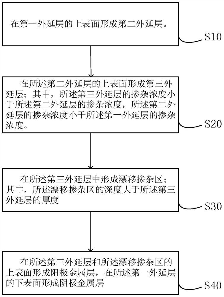
The invention belongs to the field of semiconductors, and provides a preparation method of an MPS diode and the MPS diode, and the method comprises the following steps: forming a second epitaxial layer on the upper surface of a first epitaxial layer; a third epitaxial layer is formed on the upper surface of the second epitaxial layer, the doping concentration of the third epitaxial layer is smaller than that of the second epitaxial layer, and the doping concentration of the second epitaxial layer is larger than that of the first epitaxial layer; a drift doping region is formed in the third epitaxial layer, and the depth of the drift doping region is larger than the thickness of the third epitaxial layer; and forming an anode metal layer on the upper surfaces of the third epitaxial layer and the drift doping region, and forming a cathode metal layer on the lower surface of the first epitaxial layer. When the MPS diode is turned on in the forward direction, the resistivity of the MPS diode is low, when the MPS diode is turned on in the reverse direction, the second epitaxial layer and the third epitaxial layer are in a high-resistance state, the surface electric field intensity distribution below the anode metal layer can be reduced, and the problem that the leakage current of the MPS is large is solved.

Description

technical field [0001] The application belongs to the technical field of semiconductors, and in particular relates to a method for preparing an MPS diode and the MPS diode. Background technique [0002] With the improvement of switching speed of power semiconductor devices, higher requirements are put forward for fast diodes with main power switching devices connected in parallel, clamping or buffering. The forward conduction loss is as low as possible to reduce the self-heating of the chip to achieve energy saving, and can also effectively improve the high-temperature operating characteristics of the chip. The fusion of PIN / Schottky or MPS structure can effectively solve the problem of insufficient softness of ordinary diodes. MPS diodes (Hybrid PIN / Schottky diode) is a fast recovery diode composed of an ordinary PIN diode and an increased Schottky region. In the MPS diode structure, due to the introduction of the Schottky structure, the injection efficiency of the anode is...

Claims


Application Information

Patent Timeline
IPC IPC(8): H01L29/06H01L29/872H01L21/329
CPCH01L29/872H01L29/0684H01L29/66143
Inventor 张益鸣刘杰
Owner SHENZHEN XINER SEMICON TECH CO LTD
Learn More