Eureka AIR delivers breakthrough ideas for toughest innovation challenges, trusted by R&D personnel around the world.

High-power chip heat dissipation structure and preparation method thereof

A technology for chip heat dissipation and high power. It is applied in semiconductor/solid-state device manufacturing, semiconductor/solid-state device components, and semiconductor devices. It can solve the problems of rising chip temperature, affecting chip performance, and inability to dissipate heat generated by the chip in time.

Pending Publication Date: 2022-03-29
INST OF MICROELECTRONICS CHINESE ACAD OF SCI
View PDF0 Cites 0 Cited by
  • Summary
  • Abstract
  • Description
  • Claims
  • Application Information

AI Technical Summary

Problems solved by technology

[0007] The purpose of the present invention is to provide a high-power chip heat dissipation structure and its preparation method to solve the problem that the heat diffusion layer on the front of the chip and the cooling medium directly perform heat exchange during the current heat dissipation process. The problem of the small effective heat exchange area between the working fluids makes the micro-flow heat dissipation method unable to achieve its heat dissipation effect well, and the heat generated by the chip cannot be dissipated in time, and will gather at the heat-generating junction area of ​​the chip, causing the chip temperature to rise sharply Elevated, seriously affecting the performance of the chip or even making the chip invalid

Method used


Image

  • High-power chip heat dissipation structure and preparation method thereof
  • High-power chip heat dissipation structure and preparation method thereof
  • High-power chip heat dissipation structure and preparation method thereof

Examples


Embodiment Construction

[0037] In order to clearly describe the technical solutions of the embodiments of the present invention, in the embodiments of the present invention, words such as "first" and "second" are used to distinguish the same or similar items with basically the same function and effect. For example, the first threshold and the second threshold are only used to distinguish different thresholds, and their sequence is not limited. Those skilled in the art can understand that words such as "first" and "second" do not limit the number and execution order, and words such as "first" and "second" do not necessarily limit the difference.

[0038] It should be noted that, in the present invention, words such as "exemplary" or "for example" are used as examples, illustrations or illustrations. Any embodiment or design described herein as "exemplary" or "for example" should not be construed as being preferred or advantageous over other embodiments or designs. Rather, the use of words such as "ex...


PUM


Abstract

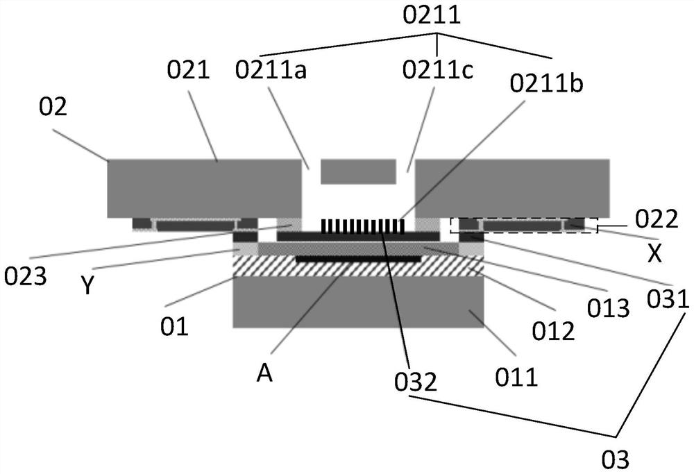
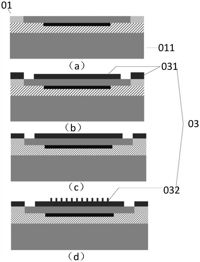
The invention discloses a high-power chip heat dissipation structure and a preparation method thereof, and relates to the technical field of microelectronic heat dissipation. The heat dissipation structure of the high-power chip comprises a heat dissipation assembly located on the high-power chip, wherein the heat dissipation assembly and the high-power chip are bonded together; the heat exchange piece located between the high-power chip and the heat dissipation assembly can lead cooling liquid to a heating junction area on the front face of the high-power chip through the heat dissipation assembly, the effective heat exchange area between the high-power chip and the heat dissipation assembly is increased through the heat exchange piece, and the heat exchange capacity is improved; the heat dissipation assembly is connected to the heat exchange piece, so that heat generated by the chip is dissipated and taken away through the front face of the chip, a heating junction area of the high-power chip can directly exchange heat with cooling liquid, the heat generated by the chip is directly conducted to the cooling liquid and then taken away through circulating flow of the cooling liquid, the heat transfer path is shortened, the heat dissipation capacity of the chip is improved, and the service life of the chip is prolonged. And the signal shielding requirement of the high-power chip and the heat dissipation requirement of the chip are met.

Description

technical field [0001] The invention relates to the technical field of microelectronic heat dissipation, in particular to a high-power chip heat dissipation structure and a preparation method thereof. Background technique [0002] With the development of semiconductor technology, the performance of semiconductor chips is constantly improving, and the power applied to the chip is also increasing, which brings about the problem of increased thermal power consumption of the chip. If the heat generated by the chip cannot be dissipated and taken away in time, it will cause The temperature of the chip rises sharply, which seriously affects the performance and life of the chip and other parameters. At the same time, the heat generation in the heat-generating junction area of ​​the chip is often uneven, which will lead to uneven temperature distribution on the chip and a large temperature gradient in the chip. On the one hand, local high-temperature hot spots will be generated, whic...

Claims


Application Information

Patent Timeline
Patent Type & Authority Applications(China)
IPC IPC(8): H01L23/473H01L23/367H01L21/50
CPCH01L23/473H01L23/367H01L21/50
Inventor 焦斌斌余立航孔延梅康玄武叶雨欣刘瑞文杜向斌贾昆鹏云世昌
Owner INST OF MICROELECTRONICS CHINESE ACAD OF SCI
Why Eureka
Eureka Blog
Learn More