Eureka AIR delivers breakthrough ideas for toughest innovation challenges, trusted by R&D personnel around the world.

Semiconductor device and manufacturing method thereof

A manufacturing method and semiconductor technology, applied in the fields of semiconductor/solid-state device manufacturing, transistors, electrical components, etc., can solve problems such as difficulties in integrating and manufacturing semiconductor devices, limiting the performance of high-voltage components, and differences in device structure requirements.

Pending Publication Date: 2022-04-01
WUHAN XINXIN SEMICON MFG CO LTD
View PDF0 Cites 0 Cited by
  • Summary
  • Abstract
  • Description
  • Claims
  • Application Information

AI Technical Summary

Problems solved by technology

The different performance requirements of high-voltage components and low-voltage components lead to large differences in device structure requirements
Using standard logic processes often limits the performance of high-voltage components
Due to high voltage requirements, high-voltage components require larger thickness of sidewalls; low-voltage components require device speed and require smaller thickness of sidewalls, making the integration and manufacture of semiconductor devices more difficult

Method used


Image

  • Semiconductor device and manufacturing method thereof
  • Semiconductor device and manufacturing method thereof
  • Semiconductor device and manufacturing method thereof

Examples


Embodiment Construction

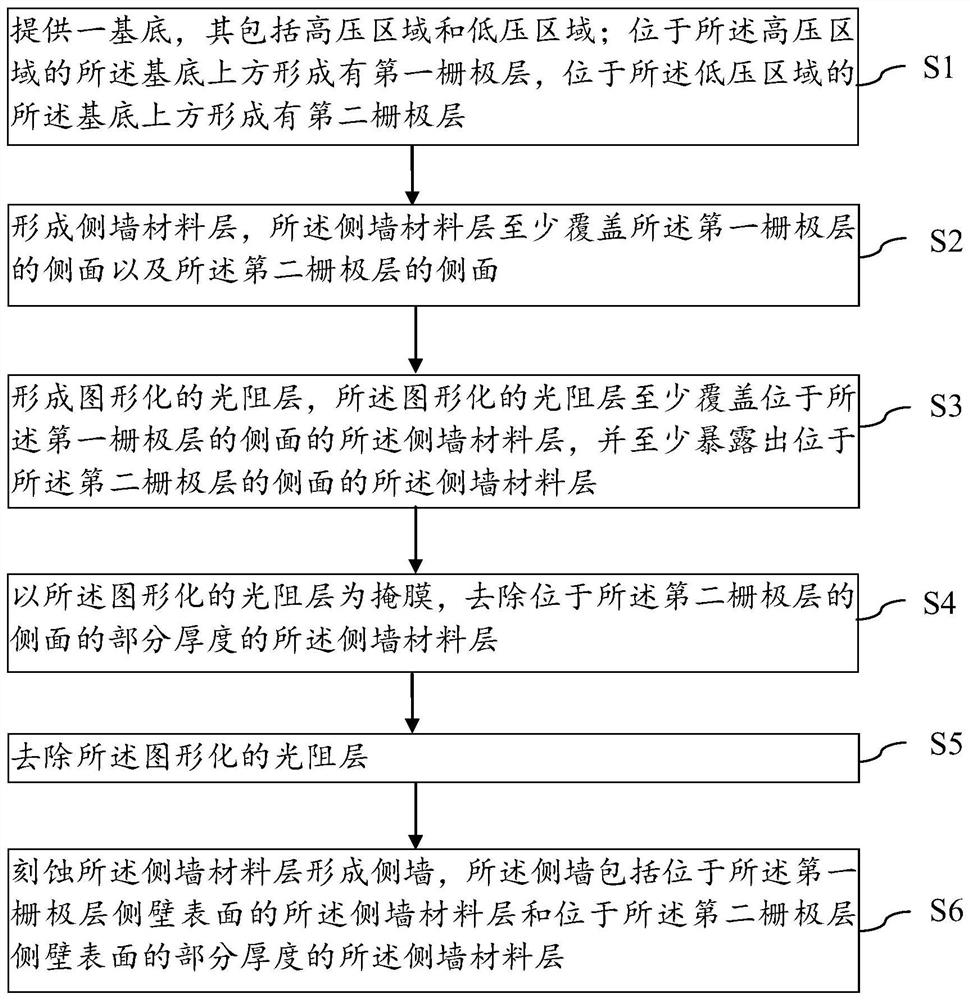
[0036] An embodiment of the present invention provides a method for manufacturing a semiconductor device. The present invention will be described in further detail below in conjunction with the accompanying drawings and specific embodiments. The advantages and features of the present invention will become clearer from the following description. It should be noted that the drawings are all in a very simplified form and use imprecise scales, and are only used to facilitate and clearly assist the purpose of illustrating the embodiments of the present invention.

[0037] An embodiment of the present invention provides a method for manufacturing a semiconductor device, such as figure 1 shown, including:

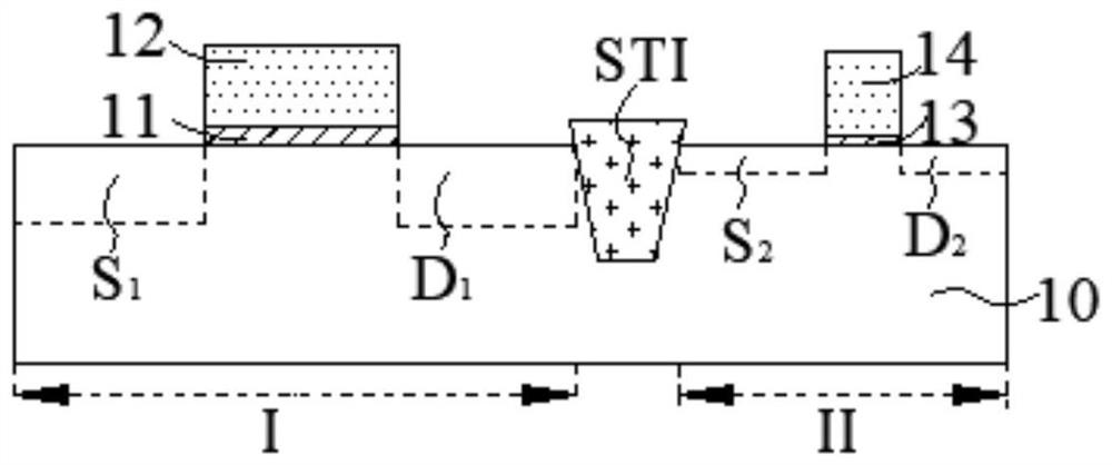
[0038] S1. A substrate is provided, which includes a high-voltage region and a low-voltage region; a first gate layer is formed on the substrate in the high-voltage region, and a second gate layer is formed on the substrate in the low-voltage region;

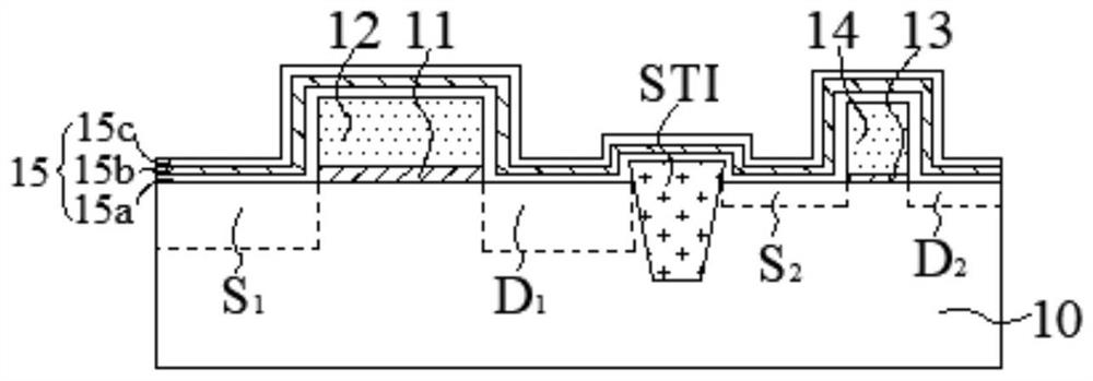
[0039] S2. Forming a side...


PUM


Abstract

The invention provides a semiconductor device and a manufacturing method thereof, and the manufacturing method comprises the steps: providing a substrate which comprises a high-voltage region and a low-voltage region; forming a side wall material layer; forming a patterned photoresist layer, and removing a partial thickness of the side wall material layer on the side surface of the second gate layer in the low-voltage region by taking the patterned photoresist layer as a mask; and etching the side wall material layer to form a side wall. A patterned photoresist layer is used as a mask to protect a side wall material layer on the side surface of a first gate layer in a high-voltage region and remove a partial thickness of the side wall material layer on the side surface of a second gate layer in a low-voltage region; therefore, when the side wall material layer is etched to form the side wall, the thickness of the side wall in the high-voltage area is larger than that of the side wall in the low-voltage area, and meanwhile, the requirements that the high-voltage element needs the side wall with the large thickness and the low-voltage element needs the side wall with the small thickness during device integration are met; and the integration feasibility of a high-voltage element and a deep submicron device is greatly improved.

Description

technical field [0001] The invention belongs to the technical field of integrated circuit manufacturing, and in particular relates to a semiconductor device and a manufacturing method thereof. Background technique [0002] In the non-standard logic process of integrated circuits, high-voltage (HV, High voltage) components are often integrated with deep submicron (28-90nm) CMOS devices (such as including low-voltage (LV, Low voltage) components), that is, integrated manufacturing in the same semiconductor device. The different performance requirements of high-voltage components and low-voltage components lead to large differences in device structure requirements. With standard logic processes, the performance of high-voltage components is often limited. Due to high voltage requirements, high-voltage components require larger thickness of sidewalls; low-voltage components require device speed and require smaller thickness of sidewalls, making the integration and manufacture ...

Claims


Application Information

Patent Timeline
IPC IPC(8): H01L21/8238H01L27/092
Inventor 程亚杰
Owner WUHAN XINXIN SEMICON MFG CO LTD
Why Eureka
Eureka Blog
Learn More