Multi-chip system of integrated antenna and manufacturing method thereof

An integrated antenna and manufacturing method technology, applied in antenna support/mounting device, semiconductor/solid-state device manufacturing, electrical components, etc., can solve the problem that antenna packaging cannot form a system-level packaging method, etc.

Pending Publication Date: 2022-04-01
NAT CENT FOR ADVANCED PACKAGING +1
View PDF0 Cites 0 Cited by
  • Summary
  • Abstract
  • Description
  • Claims
  • Application Information

AI Technical Summary

Problems solved by technology

[0008] The purpose of the present invention is to provide a multi-chip system with an integrated antenna and its manufacturing method, so as to solve the problem that the existing antenna package cannot form a system-level package

Method used


Image

  • Multi-chip system of integrated antenna and manufacturing method thereof
  • Multi-chip system of integrated antenna and manufacturing method thereof
  • Multi-chip system of integrated antenna and manufacturing method thereof

Examples


Embodiment Construction

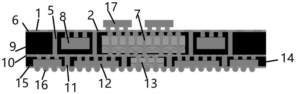
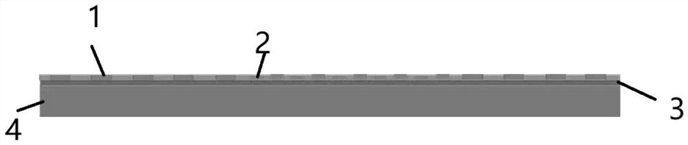
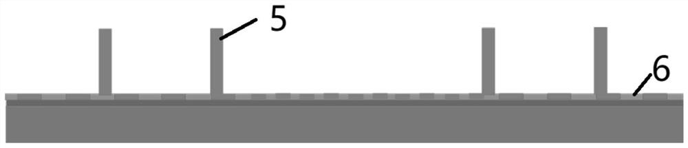
[0098] The present invention will be further described below in conjunction with specific embodiments with reference to the accompanying drawings.

[0099] It should be noted that components in the various figures may be shown exaggerated for the purpose of illustration and are not necessarily true to scale. In the various figures, identical or functionally identical components are assigned the same reference symbols.

[0100] In the present invention, unless otherwise specified, "arranged on", "arranged on" and "arranged on" do not exclude the presence of intermediates between the two. In addition, "arranged on or above" only means the relative positional relationship between two parts, and under certain circumstances, such as after the product direction is reversed, it can also be converted to "arranged under or below", and vice versa Of course.

[0101] In the present invention, each embodiment is only intended to illustrate the solutions of the present invention, and sho...


PUM


Abstract

The invention provides a multi-chip system of an integrated antenna and a manufacturing method thereof, and the system comprises a plurality of lamination layers which are configured to accommodate one or more of a plurality of chips, a superfine RDL adapter plate and a plurality of metal support columns, and the plurality of lamination layers are stacked along the thickness direction to form a vertical interconnection structure; and an intermediate RDL layer configured as an interface of the plurality of stacks.

Description

technical field [0001] The invention relates to the technical field of integrated circuits, in particular to a multi-chip system with an integrated antenna and a manufacturing method thereof. Background technique [0002] Lower cost, more reliable, faster and higher density circuits are the goals pursued by integrated circuit packaging. In the future, integrated circuit packaging will increase the integration density of various electronic components by continuously reducing the minimum feature size. [0003] Currently, advanced packaging methods include: Wafer Level Chip Scale Packaging (WLCSP), Fan-Out Wafer Level Package (FOWLP), Flip Chip, Package on Package (Package on Package, POP) and so on. [0004] Fan-out wafer-level packaging is an embedded chip packaging method for wafer-level processing. It is currently one of the advanced packaging methods with more input / output ports (I / O) and better integration flexibility. Compared with conventional wafer-level packaging, ...

Claims


Application Information

Patent Timeline
Patent Type & Authority Applications(China)
IPC IPC(8): H01L23/66H01L23/538H01L23/552H01L25/00H01L21/50H01L21/56H01Q1/22
Inventor 徐成孙鹏
Owner NAT CENT FOR ADVANCED PACKAGING
Why Eureka
Try Eureka