Anti-environment high-scattering-intensity chipless label

A scattering intensity, chipless technology, applied in the direction of recording carriers used in machines, instruments, computer components, etc., can solve problems such as difficulty in maintaining information storage and identification, chips and antennas are susceptible to interference from ambient temperature and noise, etc. Achieve high Q value, easy processing, and high spectrum utilization

Pending Publication Date: 2022-04-05
无锡众智联禾智能科技有限公司
View PDF0 Cites 0 Cited by
  • Summary
  • Abstract
  • Description
  • Claims
  • Application Information

AI Technical Summary

Problems solved by technology

With the rapid development of the Internet of Things, radio frequency identification system technology has become an important part of the Internet of Things. Traditional radio frequency identification system labels cannot replace optical barcodes due to the high cost of chips and are used on a large scale. With the complexity of the system application environment As well as the diversification of influencing factors, traditional chip radio frequency identification equipment is sometimes difficult to maintain reliable information storage and identification. The main reason is that the connection between the chip and the antenna is easily affected by the interference of ambient temperature and noise, while the stability of the connection Usually determines the performance of radio frequency identification equipment, which promotes the birth of chipless radio frequency identification technology

Method used


Image

  • Anti-environment high-scattering-intensity chipless label
  • Anti-environment high-scattering-intensity chipless label
  • Anti-environment high-scattering-intensity chipless label

Examples


Embodiment Construction

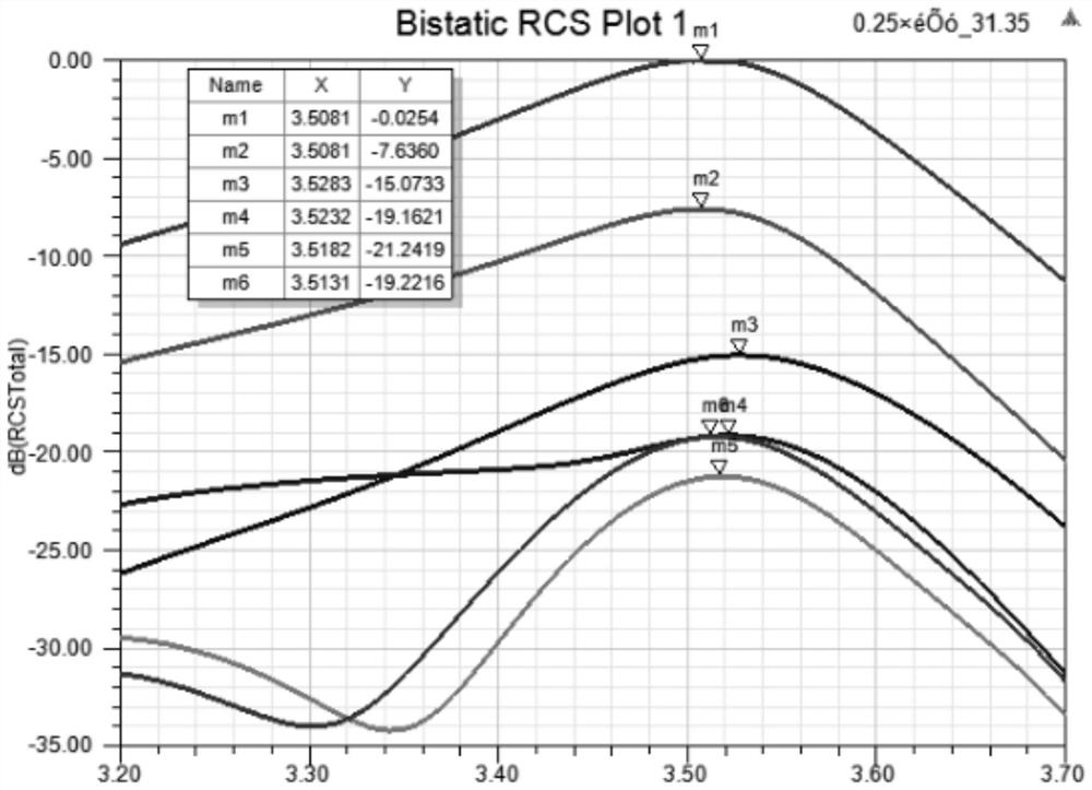
[0019] In the current popular chipless tag design, due to the limitation of the frequency band and the low quality factor of the tag itself, within a certain bandwidth, only a limited number of tags can be encoded, so in order to design with a high quality factor, within a certain bandwidth, you can As many codes as possible, so the present invention designs a chipless tag with high anti-environmental scattering intensity, combined below Figure 1 to Figure 10 The present invention will be further described.

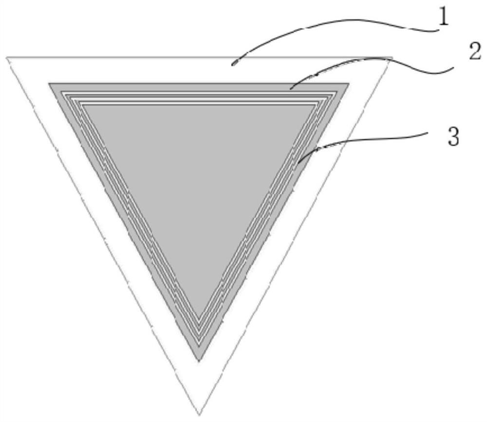
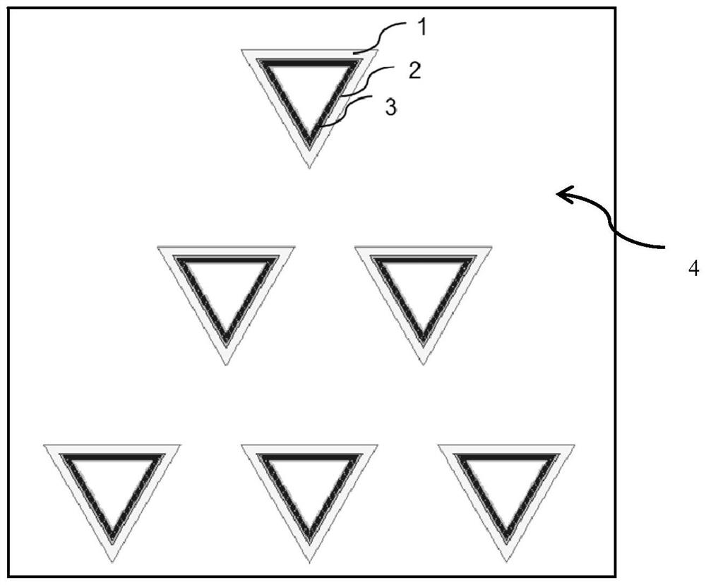
[0020] like figure 1 and figure 2 As shown, a non-chip label with high anti-environmental scattering intensity includes 6 chipless label units and a base substrate 4 . A single chipless label unit includes a dielectric layer 1 and a conductive patch layer 2 arranged on the dielectric layer 1. The conductive patch layer 2 is an equilateral triangle with a side length of 24.42 mm. There are three equilateral triangular annular slot resonators 3 , the width of each slot...


PUM

PropertyMeasurementUnit
lengthaaaaaaaaaa
thicknessaaaaaaaaaa
lengthaaaaaaaaaa

Abstract

The invention discloses an environment-resistant chip-free tag with high scattering intensity, and relates to the field of electronic tags. Comprising a plurality of chip-free tag units and a substrate, each chip-free tag unit comprises a dielectric layer and a conductive patch layer arranged on the dielectric layer, the conductive patch layer is provided with a plurality of triangular annular gap resonant cavities, and the resonant frequency is adjusted by changing the lengths of the triangular annular gap resonant cavities. The plurality of chip-free label units are arranged on the substrate in a triangular distribution mode. The tag has the advantages that the designed triangular resonance structure is directly utilized, so that the tag has the characteristic of insensitivity to the polarization direction and has a higher Q value. In a 100MHz frequency band of 3.45-3.55 GHz, three or more label codes can be realized, and the frequency spectrum utilization rate is higher. The utilization rate of the label medium substrate is higher, and higher coding capacity can be realized in a smaller size, namely, the data capacity density is higher. The label is simpler in structural design and easier to process.

Description

technical field [0001] The invention relates to the field of electronic tags, in particular to a non-chip tag with high anti-environmental scattering intensity. Background technique [0002] The chipless tag uses the read-write antenna to send a broadband scanning frequency signal, and then captures the backscatter signal of the tag on the receiving antenna, which has the characteristics of low power consumption and simple structure. Due to the radio frequency integrated IC in the traditional chip RFID tag Very expensive, and chipless RFID tags do not contain radio frequency integrated IC. Moreover, compared with traditional RFID tags, chipless RFID tags do not carry any electronic circuits used to process communication protocols in their structure, which effectively reduces the manufacturing cost of chipless RFID. Chipless RFID tags can independently complete the functions of transmitting and receiving electromagnetic waves and encoding, which makes the manufacturing proce...

Claims


Application Information

Patent Timeline
Patent Type & Authority Applications(China)
IPC IPC(8): G06K19/077
Inventor 冷利忠付高岩冷涛
Owner 无锡众智联禾智能科技有限公司
Why Eureka
Try Eureka