Ultrahigh-integration multi-path parallel photoelectric conversion assembly

A photoelectric conversion and component technology, applied in the direction of electrical components, electrical solid devices, circuits, etc., can solve the problems of poor multi-channel integration isolation, complex structure, poor link index, etc., to improve reliability and performance indicators, Reduce the difficulty of system structure and improve the effect of channel isolation

Pending Publication Date: 2022-04-05
CHINA AVIATION OPTICAL-ELECTRICAL TECH CO LTD
View PDF0 Cites 1 Cited by
  • Summary
  • Abstract
  • Description
  • Claims
  • Application Information

AI Technical Summary

Problems solved by technology

[0004] 1) At present, microwave signal optical transmission technology is still based on discrete devices, and the integration is extremely low, which makes it difficult for the entire system to exert its potential advantages in terms of comprehensive performance level, volume, weight, power consumption, and cost, and cannot adapt to rapid development. Optical transmission technology application requirements;
[0005] 2) The isolation degree is poor during multi-channel integration. Electronic countermeasures, radar communication and other fields have relatively high requirements for volume, quality, and isolation. When multiple photodetectors and radio frequency amplifiers are integrated in a small space, it cannot meet the requirements. High isolation requirements;
[0006] 3) Poor reliability and performance indicators: Using the existing technology to realize the optical transmission of microwave signals, the hardware is difficult, the structure is complex, and the interconnection of multiple devices is difficult, which reduces the reliability of the entire system
In addition, the link index is poor when based on discrete devices, for example, the in-band flatness of 0.8-18GHz is generally ±3dB

Method used


Image

  • Ultrahigh-integration multi-path parallel photoelectric conversion assembly
  • Ultrahigh-integration multi-path parallel photoelectric conversion assembly
  • Ultrahigh-integration multi-path parallel photoelectric conversion assembly

Examples


Embodiment Construction

[0031] In order to better understand the content of the present invention, the present invention will be further described below in conjunction with specific embodiments and accompanying drawings. The following examples are implemented based on the technology of the present invention, providing detailed implementation and operation steps, but the protection scope of the present invention is not limited to the following examples.

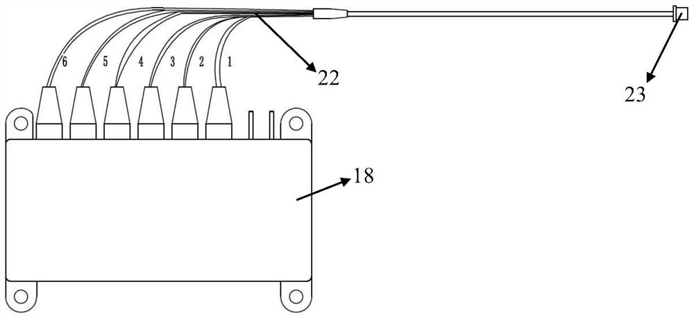
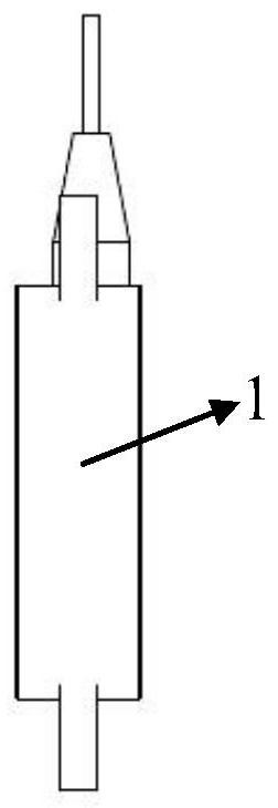
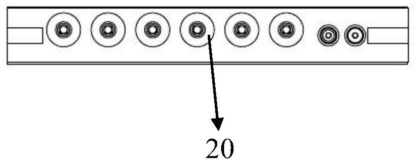
[0032] Existing microwave optoelectronic device detectors and amplifiers have their own specific packaging technology, and the interconnection and integration of the two packaging forms are relatively difficult, which does not meet the needs of the new generation of weapons and equipment. The invention integrates different types of PIN photoelectric chips (detector chips) and radio frequency microwave chips for the first time through impedance matching by using micro-assembly technology, and multi-channel integration realizes miniaturization and high ...


PUM


Abstract

The invention relates to an ultra-high integrated multipath parallel photoelectric conversion assembly, which comprises an outer shell, and a power supply protection circuit board, a power supply wiring board and a plurality of integrated cavities which are arranged in the outer shell, and is characterized in that each integrated cavity is internally provided with a detector chip, a radio frequency amplifier and a radio frequency adjustable attenuator; in each integrated cavity, the detector chip is connected with an optical coupling system at the top of the cavity, and the radio frequency adjustable attenuator is connected with an SSMP connector arranged at the bottom of the cavity; the radio frequency amplifier is arranged between the detector chip and the radio frequency adjustable attenuator; the detector chip and the radio frequency amplifier, the radio frequency amplifier and the radio frequency adjustable attenuator, and the radio frequency adjustable attenuator and the SSMP connector are connected through microstrip lines. In combination with the advantages of high bandwidth, low loss, interference resistance and the like of microwave light, the detector, the amplifier and the attenuator are mixed and integrated in multiple paths by adopting a micro-assembly technology, and the device has the characteristics of super miniaturization, high integration level, adjustable attenuation, high reliability and the like.

Description

technical field [0001] The invention relates to the technical field of photoelectric conversion, in particular to an ultra-highly integrated multi-channel parallel photoelectric conversion component. Background technique [0002] Radio frequency optical transmission is one of the important applications of microwave photonics. With the rapid development of microwave communication and optical fiber communication, microwave communication has defects in long-distance transmission and large-capacity transmission, which has led to the optical fiber transmission technology of microwave signals, namely Radio over Fiber (ROF) technology. Microwave optical transmission technology has the advantages of low loss, large bandwidth, light weight, anti-interference and wavelength division multiplexing, which effectively overcomes the defects of microwave communication. However, low cost, high performance and arraying have become one of the technical bottlenecks limiting the application of ...

Claims


Application Information

Patent Timeline
Patent Type & Authority Applications(China)
IPC IPC(8): H01L25/16H01L23/66H04B10/70
Inventor 张江帆左朋莎任欢许利伟宋春峰
Owner CHINA AVIATION OPTICAL-ELECTRICAL TECH CO LTD
Why Eureka
Try Eureka