Ferroelectric memristor based on lanthanum titanate and preparation method thereof
A technology of memristive devices and lanthanum titanate, which is applied in the field of ferroelectric memristive devices based on lanthanum titanate and its preparation, can solve urgent research problems and achieve the effect of simple preparation method, low cost, and widening application scenarios
- Summary
- Abstract
- Description
- Claims
- Application Information
AI Technical Summary
Problems solved by technology
Method used
Image


Examples
Embodiment 1
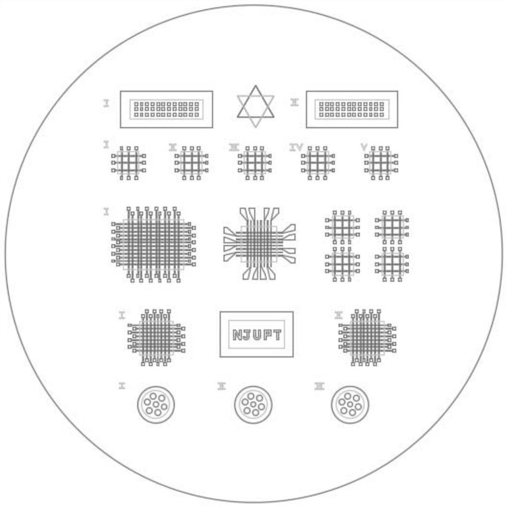
[0039] Such as figure 1 As shown, a ferroelectric memristive device based on lanthanum titanate, the ferroelectric memristive device is arranged on the substrate, and the ferroelectric memristive device includes a bottom electrode, a resistive layer and a The top electrode, the material of the bottom electrode and the top electrode is TiN, and the material of the resistive layer is La 2 Ti 2 o 7 ; The bottom surface of the resistive switch layer is in contact with the top surface of the bottom electrode, the top surface of the resistive switch layer is in contact with the bottom surface of the top electrode, and the ferroelectric memristive device is integrated with an NJUPT in one area A single device with lettering, a rectangular single device with 2 regions, a circular single device with 3 regions, 9 3×3 memristor arrays, 3 8×8 memristor arrays, and 1 12×12 memristor array.
[0040] In some embodiments, the bottom electrode, the resistive switch layer and the top electr...
Embodiment 2
[0047] A method for preparing a ferroelectric memristive device based on lanthanum titanate, the method includes two parts:
[0048] 1. Design a new type of mask, and the device types include: a single device with NJUPT in 1 area, a rectangular single device in 2 areas, a circular single device in 3 areas, 9 3×3 memristor arrays, 3 8×8 memristor array, 1 12×12 memristor array.
[0049]2. Prepare a ferroelectric memristive device based on lanthanum titanate, comprising the following steps:
[0050] S1: Clean the silicon wafer with deionized water and then dry it with a dryer, and cover the dried silicon wafer with the first mask (such as figure 2 shown), through PVD physical vapor deposition, a layer of TiN with a thickness of 100 nm was deposited under vacuum as the bottom electrode;
[0051] S2: Remove the first mask and cover the second mask with alignment marks (such as image 3 shown), a layer of La with a thickness of 20nm was oxidized and grown under vacuum 2 Ti 2 ...
PUM
| Property | Measurement | Unit |
|---|---|---|
| thickness | aaaaa | aaaaa |
| thickness | aaaaa | aaaaa |
Abstract
Description
Claims
Application Information
 - R&D
- Intellectual Property
- Life Sciences
- Materials
- Tech Scout
- Unparalleled Data Quality
- Higher Quality Content
- 60% Fewer Hallucinations
Browse by: Latest US Patents, China's latest patents, Technical Efficacy Thesaurus, Application Domain, Technology Topic, Popular Technical Reports.
© 2025 PatSnap. All rights reserved.Legal|Privacy policy|Modern Slavery Act Transparency Statement|Sitemap|About US| Contact US: help@patsnap.com