Photoetching splicing error detection method, two-dimensional grating manufacturing method and mask plate

A detection method and mask technology, applied in the field of integrated circuits, can solve problems such as lithographic splicing errors, and achieve the effect of avoiding splicing errors and ensuring integrity

Active Publication Date: 2022-04-08
SHANGHAI INTEGRATED CIRCUIT EQUIP & MATERIALS IND INNOVATION CENT CO +1
View PDF6 Cites 2 Cited by
  • Summary
  • Abstract
  • Description
  • Claims
  • Application Information

AI Technical Summary

Problems solved by technology

[0005] The object of the present invention is to provide a method for detecting lithographic splicing errors, a method for manufacturing a two-dimensional grating and a mask plate, so as to solve the problem of lithographic splicing errors that occur in grating manufacturing

Method used


Image

  • Photoetching splicing error detection method, two-dimensional grating manufacturing method and mask plate
  • Photoetching splicing error detection method, two-dimensional grating manufacturing method and mask plate
  • Photoetching splicing error detection method, two-dimensional grating manufacturing method and mask plate

Examples


Embodiment Construction

[0041] The method for detecting splicing errors in lithography, the method for manufacturing a two-dimensional grating, and the mask plate proposed by the present invention will be further described in detail below with reference to the accompanying drawings and specific embodiments. Advantages and features of the present invention will be apparent from the following description and claims. It should be noted that all the drawings are in a very simplified form and use imprecise scales, and are only used to facilitate and clearly assist the purpose of illustrating the embodiments of the present invention.

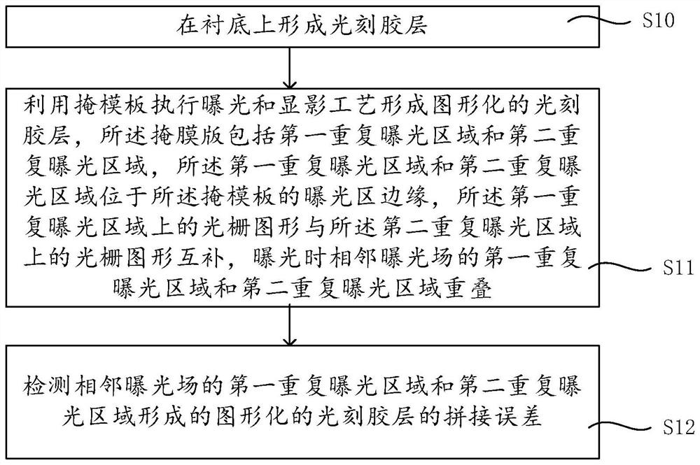
[0042] figure 1 It is a flow chart of a method for detecting a photolithography splicing error according to an embodiment of the present invention. Such as figure 1 As shown, an embodiment of the present invention provides a method for detecting a photolithography splicing error, including:

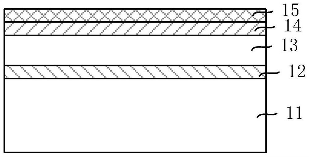
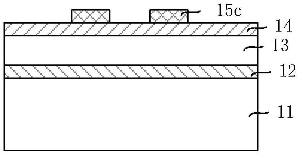
[0043] Step S10, forming a photoresist layer on the substrate;

[0044] Step S1...


PUM


Abstract

The invention provides a photoetching splicing error detection method, a two-dimensional grating manufacturing method and a mask plate. The photoetching splicing error detection method comprises the following steps: forming a photoresist layer on a substrate; a mask plate is used for executing exposure and development processes to form a graphical photoresist layer, the mask plate comprises a first repeated exposure area and a second repeated exposure area, and the first repeated exposure area and the second repeated exposure area are located on the edge of the exposure area of the mask plate. The grating pattern on the first repeated exposure area and the grating pattern on the second repeated exposure area are complementary, and the first repeated exposure area and the second repeated exposure area of adjacent exposure fields are overlapped during exposure; and detecting splicing errors of the patterned photoresist layers formed in the first repeated exposure region and the second repeated exposure region of the adjacent exposure fields by utilizing defect scanning equipment. According to the splicing error detection result, the position, direction and size of the splicing error of the two-dimensional grating can be determined, process correction is carried out, and the splicing error of the two-dimensional grating is avoided.

Description

technical field [0001] The invention relates to the technical field of integrated circuits, in particular to a method for detecting splicing errors in photolithography, a method for manufacturing a two-dimensional grating, and a mask. Background technique [0002] Gratings are widely used in high-precision measurement, especially the current integrated circuits, precision machining, microscopic technology, etc. have put forward higher requirements for accurate measurement of position. The measurement systems in these fields need to accurately measure and position the two-dimensional direction of the worktable. Taking semiconductor equipment as an example, the lithography machine used for advanced manufacturing uses two-dimensional gratings to realize the nanometer precision of the workpiece table in the long stroke. Level precise positioning, which means that the grating itself needs to achieve extremely high manufacturing accuracy. [0003] The traditional grating manufact...

Claims


Application Information

Patent Timeline
Patent Type & Authority Applications(China)
IPC IPC(8): G03F7/20G03F1/44G02B5/18
CPCY02P70/50
Inventor 刘谆骅袁伟
Owner SHANGHAI INTEGRATED CIRCUIT EQUIP & MATERIALS IND INNOVATION CENT CO
Why Eureka
Try Eureka