
Method for processing CIS (Contact Image Sensor) wafer by utilizing grid type glass carrier plate

A glass and wafer technology, applied in the field of processing CIS wafers using grid-type glass carrier discs, can solve the problems of easy warpage, low yield, waste, etc., to improve yield, save process costs, and overcome process problems. The effect of restriction

Pending Publication Date: 2022-04-15
绍兴同芯成集成电路有限公司
View PDF0 Cites 0 Cited by
  • Summary
  • Abstract
  • Description
  • Claims
  • Application Information

AI Technical Summary

Problems solved by technology

However, when the CIS glass cover is thinned, it is prone to warping and cannot be laminated with Wafer. When the traditional operation method can only select qualified products with small warpage after the CV process for lamination, the yield rate is low, resulting in a lot of waste.

Method used


Image

  • Method for processing CIS (Contact Image Sensor) wafer by utilizing grid type glass carrier plate
  • Method for processing CIS (Contact Image Sensor) wafer by utilizing grid type glass carrier plate
  • Method for processing CIS (Contact Image Sensor) wafer by utilizing grid type glass carrier plate

Examples


Embodiment Construction

[0025] The following will clearly and completely describe the technical solutions in the embodiments of the present invention with reference to the accompanying drawings in the embodiments of the present invention. Obviously, the described embodiments are only some, not all, embodiments of the present invention. Based on the embodiments of the present invention, all other embodiments obtained by persons of ordinary skill in the art without creative efforts fall within the protection scope of the present invention.

[0026] In describing the present invention, it is to be understood that the terms "opening", "upper", "lower", "thickness", "top", "middle", "length", "inner", "surrounding" etc. Indicating orientation or positional relationship is only for the convenience of describing the present invention and simplifying the description, and does not indicate or imply that the components or elements referred to must have a specific orientation, be constructed and operated in a sp...


PUM


Abstract

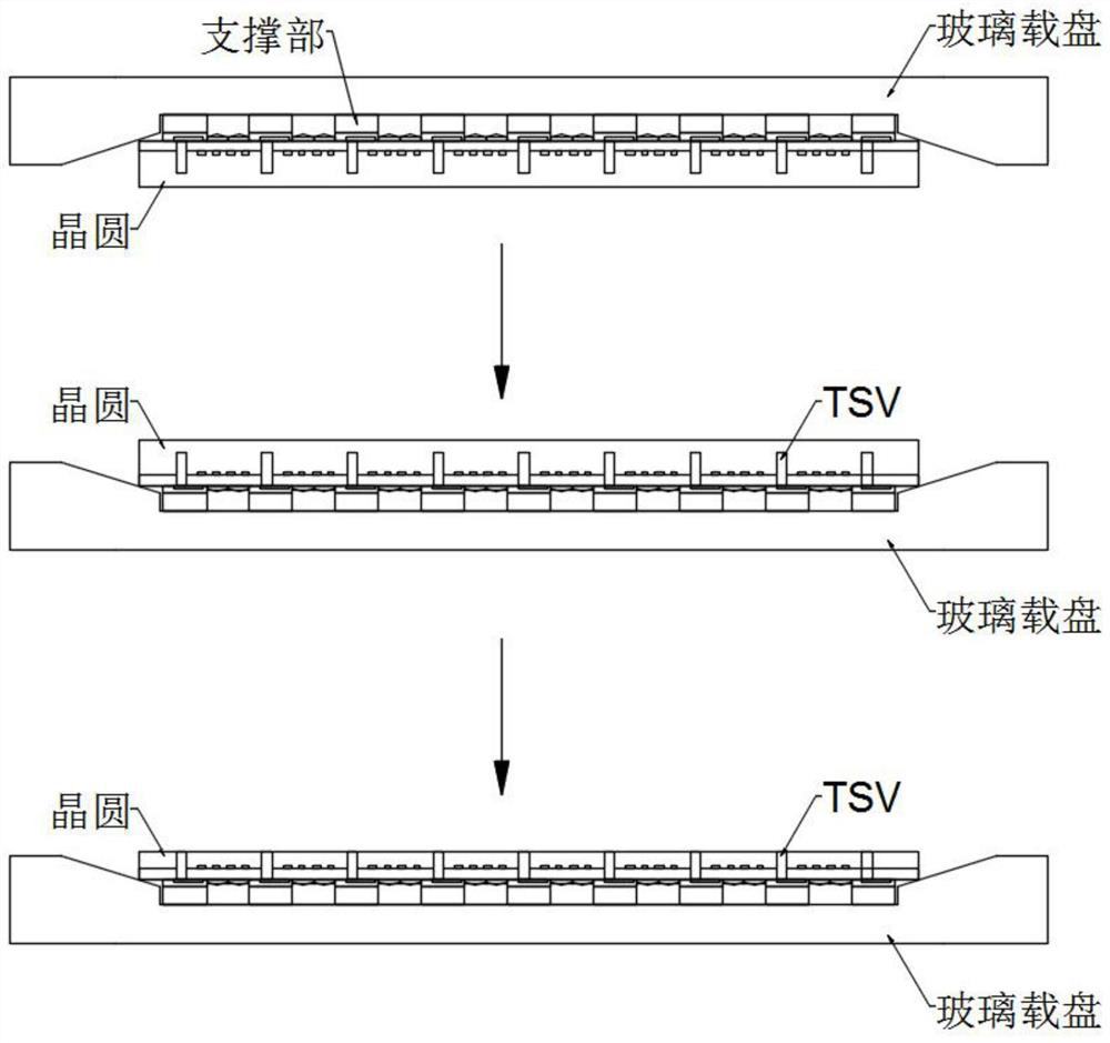
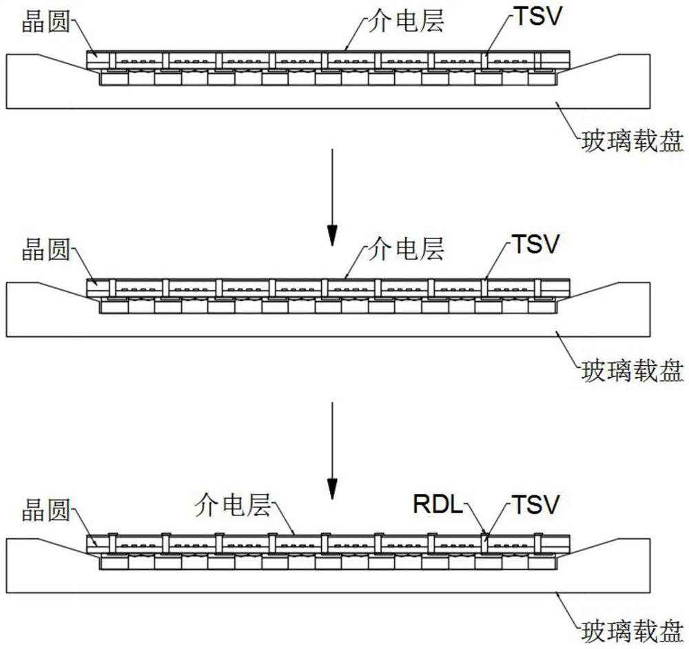
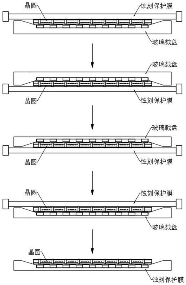
The invention discloses a method for processing a CIS wafer by using a grid-type glass carrier plate, and the method comprises the following steps: S1, bonding the front surface of the wafer with the grid-type glass carrier plate, and carrying out the thinning of the back surface of the wafer until a TSV is exposed; s2, depositing a dielectric layer on the back surface of the wafer, and then forming a redistribution line (RDL) and a welding spot through chemical plating; s3, attaching an etching protection film to the back surface of the wafer, thinning the whole glass carrying disc, and then tearing and lifting the etching protection film; s4, performing chemical plating on the surface of the RDL to form a pre-welding layer, and then welding a metal column; and S5, cutting to remove the edges of the wafer and the glass carrier plate to obtain the processed CIS wafer. According to the invention, a polymer bonding block between a glass cover and a wafer in the traditional CIS process is replaced by the grid-type glass carrier plate supporting part, so that the process limitation that the glass carrier plate is not resistant to high temperature and cannot be soaked in acid for a long time is overcome, and meanwhile, after the glass carrier plate is thinned, the edge of the carrier plate and the supporting part still have certain thickness; therefore, stress support during thinning of the back of the wafer is met.

Description

technical field [0001] The invention relates to the field, in particular to a method for processing a CIS wafer by using a grid type glass carrier. Background technique [0002] Microelectronic imaging components are widely used in mobile devices, and image sensors are an important part of microelectronic imaging components. Image sensors are semiconductor devices that convert optical images into electrical signals, and can generally be divided into charge-coupled devices (CCD) and complementary Metal oxide semiconductor image sensor chip (CMOS image sensor chip, CIS). [0003] The CIS chip uses the control circuit and the signal processing circuit located around the MOS transistor and uses the switching technology of the MOS transistor to sequentially detect the output. The number of MOS transistors is equal to the number of pixels. To the photosensitive area on the chip, the conversion of optical signal to electrical signal is completed, thus the principle of imaging. Th...

Claims


Application Information

Patent Timeline
Patent Type & Authority Applications(China)
IPC IPC(8): H01L27/146
Inventor 严立巍符德荣陈政勋
Owner 绍兴同芯成集成电路有限公司
Learn More