MEMS built-in chip packaging carrier and manufacturing process thereof

A technology for encapsulating carrier boards and manufacturing processes, which is applied in the fields of producing decorative surface effects, decorative arts, and metal material coating processes, etc., and can solve the problems of inability to implement built-in chips, poor packaging and shielding effects, and low signal-to-noise ratio of products problems such as improving sensitivity and signal-to-noise ratio, reducing interference, and increasing volume

Pending Publication Date: 2022-04-19
JIANGSU PROVISION ELECTRONICS CO LTD
View PDF0 Cites 2 Cited by
  • Summary
  • Abstract
  • Description
  • Claims
  • Application Information

AI Technical Summary

Problems solved by technology

At present, some MEMS carrier boards are made by overlapping three-layer PCB boards. The three-layer PCB boards are laminated to form a cavity, and the metal surface is plated on the second layer PCB board to form a shielding cavity. This package has poor shielding effect. The volume of the back cavity is small, the signal-to-noise ratio of the product is low, and the built-in chip cannot be realized

Method used


Image

  • MEMS built-in chip packaging carrier and manufacturing process thereof
  • MEMS built-in chip packaging carrier and manufacturing process thereof
  • MEMS built-in chip packaging carrier and manufacturing process thereof

Examples


Embodiment

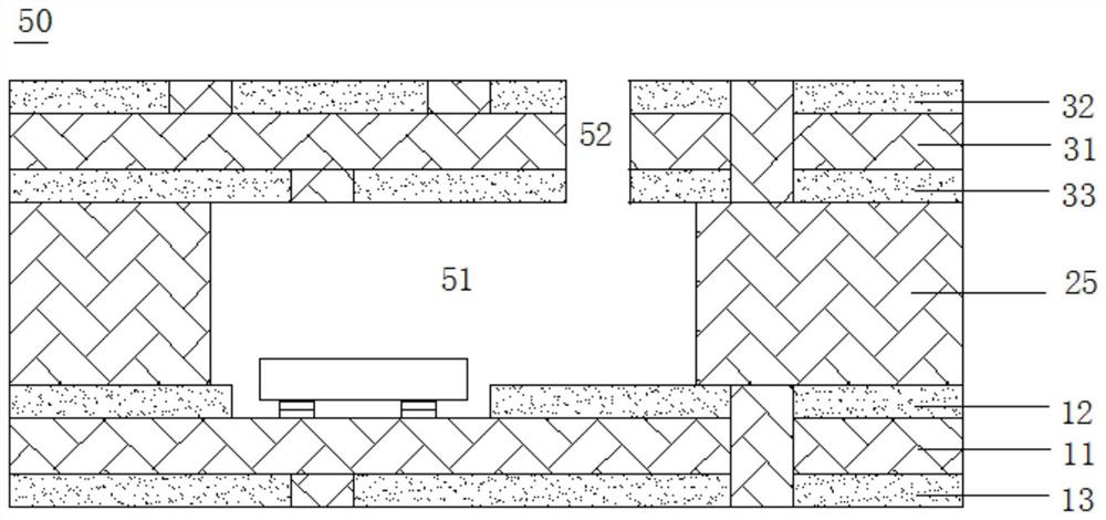
[0060] Example: such as Figure 1-12 As shown, a manufacturing process of a MEMS built-in chip package carrier plate includes the following steps:

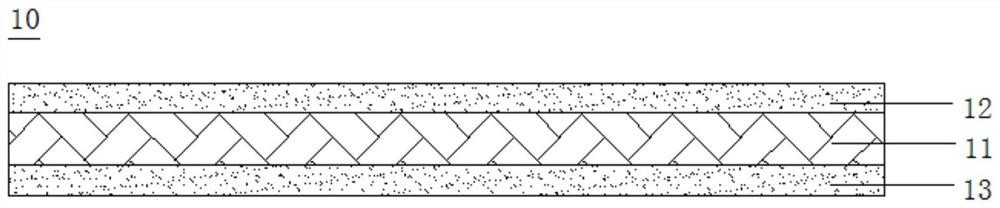
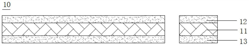
[0061] Step 1: Prepare three core boards, namely the first core board 10, the second core board 20 and the third core board 30, wherein, as figure 2 As shown, the first core board 10 includes a first insulating layer 11 and a first copper foil layer 12 and a second copper foil layer 13 respectively arranged on the front and back sides of the capacitance layer, as shown in Figure 6 As shown, the second core board 20 includes a second insulating layer 21 and a third copper foil layer 22 and a fourth copper foil layer 23 respectively disposed on the front and back sides of the second insulating layer, as shown in Figure 9 As shown, the third core board 30 includes a third insulating layer 31 and a fifth copper foil layer 32 and a sixth copper foil layer 33 respectively disposed on the front and back sides of the third insulating ...


PUM


Abstract

The invention relates to an MEMS built-in chip packaging carrier plate and a manufacturing process thereof, and the process comprises the following steps: preparing three core plates, namely a first core plate, a second core plate and a third core plate, and drilling and filling holes in the first core plate; an inner layer circuit of the first core board; sMT surface mounting is carried out; etching a second core plate and pressing a film; grooving the film plate; drilling and hole filling of the third core board; an inner layer circuit of the third core board; pressing: pressing the first core plate, the film plate and the third core plate together; and opening the cover. According to the packaging substrate, the function of a built-in chip is achieved, the size of the back cavity is increased under the condition that the size of a device is not increased, the sensitivity and the signal-to-noise ratio of a product are improved, and the packaging substrate conforms to the development trend of device miniaturization.

Description

technical field [0001] The invention relates to a MEMS packaging carrier board, in particular to a MEMS built-in chip packaging carrier board and a manufacturing process thereof. Background technique [0002] The development of MEMS (Microelectromechanical Systems) technology and process in the past three decades, especially the development of MEMS technology based on silicon chips, has realized the miniaturization and low cost of many sensors (such as pressure sensors, accelerometers, gyroscopes, etc.). At present, some MEMS carrier boards are made by overlapping three-layer PCB boards. The three-layer PCB boards are laminated to form a cavity, and the metal surface is plated on the second layer PCB board to form a shielding cavity. This package has poor shielding effect. The volume of the back cavity is small, the signal-to-noise ratio of the product is low, and the built-in chip cannot be realized. Contents of the invention [0003] In order to overcome the above-menti...

Claims


Application Information

Patent Timeline
IPC IPC(8): B81C1/00B81B7/00B81B7/02
CPCB81C1/00047B81C1/00261B81B7/0032B81B7/02
Inventor 马洪伟张志礼
Owner JIANGSU PROVISION ELECTRONICS CO LTD
Why Eureka
Try Eureka