Monocrystalline silicon wafer cleaning equipment

A technology for cleaning equipment and single crystal silicon wafers, which is applied in the directions of cleaning methods, cleaning methods and utensils, chemical instruments and methods using liquids, etc. To achieve the effect of improving cleaning efficiency and easy adjustment

Inactive Publication Date: 2022-04-22
无锡京运通科技有限公司
View PDF8 Cites 2 Cited by
  • Summary
  • Abstract
  • Description
  • Claims
  • Application Information

AI Technical Summary

Problems solved by technology

[0003] However, when the existing ultrasonic cleaning machine is in use, the operator needs to clean the silicon wafer several times, because the operation steps of taking the silicon wafer back and forth from the cleaning box and placing it in the new cleaning box are cumbersome, which is not conducive to Improve the cleaning speed of silicon wafers; in addition, the silicon wafers are placed directly in the cleaning box for cleaning, because the parts where multiple silicon wafers are stacked together are not easy to clean in place, and impurities are easy to adhere to the silicon wafers after cleaning. To a certain extent, it is not conducive to improving the cleaning effect of silicon wafers

Method used


Image

  • Monocrystalline silicon wafer cleaning equipment
  • Monocrystalline silicon wafer cleaning equipment
  • Monocrystalline silicon wafer cleaning equipment

Examples


Embodiment Construction

[0025] In order to make the technical means, creative features, goals and effects achieved by the present invention easy to understand, the present invention will be further described below in conjunction with specific embodiments.

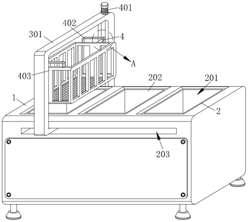
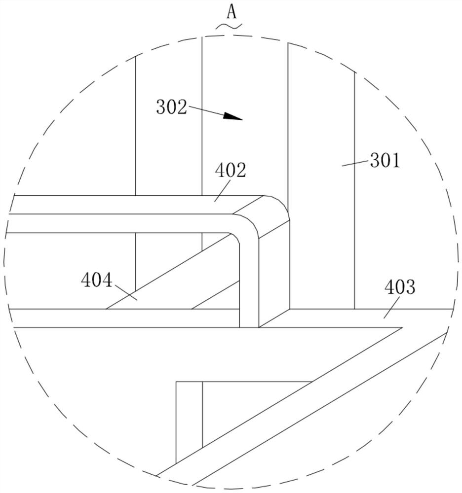
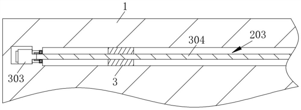
[0026] Such as Figure 1-Figure 8 As shown, a cleaning device for monocrystalline silicon wafers according to the present invention includes a cleaning machine body 1, and a main body mechanism 2 is connected to the cleaning machine body 1; an adjusting mechanism 3 is fitted on the cleaning machine body 1 A storage mechanism 4 is installed on the adjustment mechanism 3; a shaking mechanism 5 is slid on the storage mechanism 4; a conflicting mechanism 6 is provided on the washing machine body 1 for cooperation and rotation;

[0027] The interference mechanism 6 includes a third motor 601, the washing machine body 1 is fixedly installed with a third motor 601, the output end of the third motor 601 is fixedly connected with a rotating shaft 602 throu...


PUM


Abstract

The invention relates to the technical field of monocrystalline silicon wafers, in particular to monocrystalline silicon wafer cleaning equipment which comprises a cleaning machine body connected with a main body mechanism. An adjusting mechanism is arranged on the cleaning machine body in a matched and sliding mode. A storage mechanism is mounted on the adjusting mechanism; a shaking mechanism slides on the storage mechanism; an abutting mechanism is rotationally arranged on the cleaning machine body in a matched mode. The adjusting mechanism is opened, so that the adjusting mechanism slides in the cleaning machine body, and the monocrystalline silicon wafer can be cleaned for multiple times through the adjusting mechanism; the storage mechanism slides into the main body mechanism from the adjusting mechanism, so that the monocrystalline silicon wafers in the storage mechanism can be conveniently cleaned when the cleaning machine body is started; an operator turns on a control switch of the abutting mechanism, so that the abutting mechanism abuts against the storage mechanism in the main body mechanism when rotating, the storage mechanism drives the shaking mechanism to slide when being abutted, and the cleaning effect of the monocrystalline silicon wafer is improved conveniently when the silicon wafer shakes in the storage mechanism.

Description

technical field [0001] The invention relates to the technical field of monocrystalline silicon wafers, in particular to a cleaning device for monocrystalline silicon wafers. Background technique [0002] Single crystal silicon usually refers to a substance formed by an arrangement of silicon atoms. Silicon is the most common and widely used semiconductor material. When molten elemental silicon solidifies, silicon atoms are arranged in a diamond lattice to form crystal nuclei, and the crystal nuclei grow into crystal grains with the same crystal plane orientation, forming single crystal silicon. When cleaning monocrystalline silicon wafers, operators generally use ultrasonic cleaning machines to clean particles, organic matter and other impurities on the surface of polycrystalline silicon wafers. [0003] However, when the existing ultrasonic cleaning machine is in use, the operator needs to clean the silicon wafer several times, because the operation steps of taking the sil...

Claims


Application Information

Patent Timeline
Patent Type & Authority Applications(China)
IPC IPC(8): B08B3/12B08B13/00
CPCB08B3/12B08B13/00
Inventor 朱仁德章祥静
Owner 无锡京运通科技有限公司
Why Eureka
Try Eureka