Device and method for testing frequency response of electro-optic intensity modulator chip

A technology of electro-optical intensity modulation and frequency response testing, applied in frequency measurement devices, electronic circuit testing and other directions, can solve problems such as result deviation, and achieve the effect of eliminating uneven ground response

Active Publication Date: 2022-04-29
UNIV OF ELECTRONICS SCI & TECH OF CHINA
View PDF11 Cites 2 Cited by
  • Summary
  • Abstract
  • Description
  • Claims
  • Application Information

AI Technical Summary

Problems solved by technology

[0004] Many of the above test methods are mainly for discrete devices that have been packaged and molded. For chip test scenarios, due to the impact of impedance mismatch, there is a gap between the microwave signal power output by the microwave signal source and the microwave power actually loaded on the modulator chip for modulation. Large differences, the results obtained by general test methods will have large deviations

Method used


Image

  • Device and method for testing frequency response of electro-optic intensity modulator chip
  • Device and method for testing frequency response of electro-optic intensity modulator chip
  • Device and method for testing frequency response of electro-optic intensity modulator chip

Examples


Embodiment

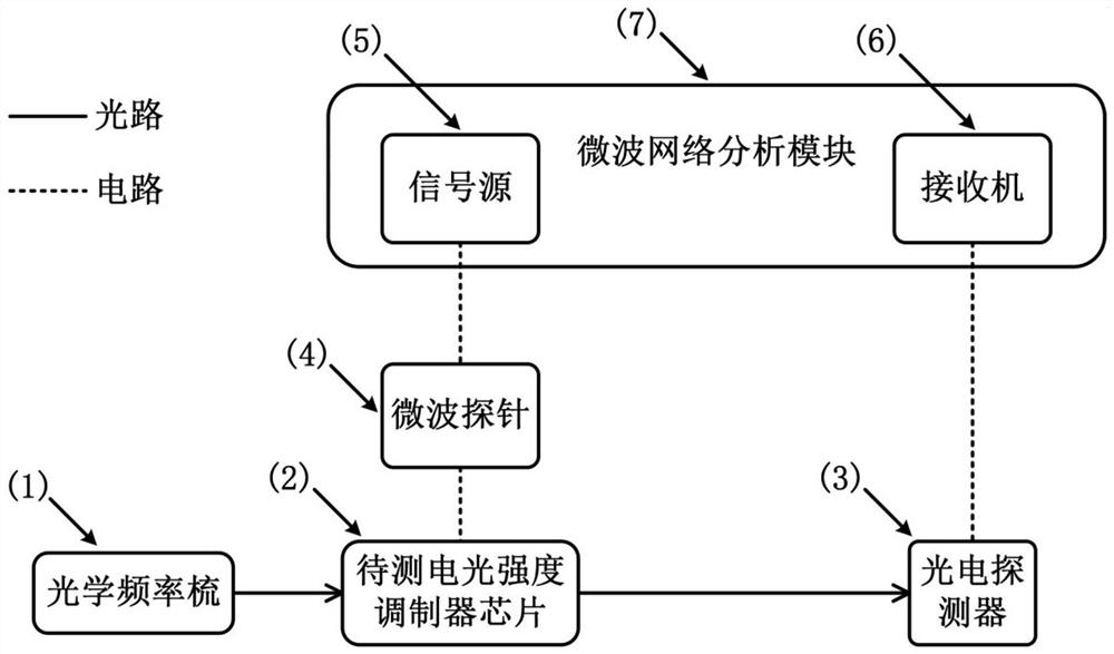
[0041] In this embodiment, a passively mode-locked fiber laser is used as an optical frequency comb source, and it is measured that the repetition frequency of the pulsed light emitted by it is 21.939 MHz, the central wavelength of the light is about 1559 nm, and the 3-dB spectral width is 0.9 nm. It can be seen that the scanning frequency step size of the test is f r =21.939MHz, the frequency point of the signal source output sweep signal of the microwave network analysis module is set as: f'(n)=nf r / 2-0.5MHz (n=1,2,3...,1140), the sweep frequency range is about 10MHz~12.5GHz, at this time, the receiving frequency of the receiver of the microwave network analysis module is set at f’(n) and nf r -f'(n), sequentially measure the magnitude spectrum P[f'(n)] and P[nf of two sets of electrical signals r -f’(n)], according to the formula (1), the uneven response K(nf r ). If the signal source output power of the microwave network analysis module is set to be a frequency sweep s...


PUM

PropertyMeasurementUnit
wavelengthaaaaaaaaaa

Abstract

The invention discloses a device and a method for testing the frequency response of a chip of an electro-optic intensity modulator, belongs to the technical field of photoelectronics, and aims to realize the intrinsic frequency response test of a bare chip of the electro-optic intensity modulator. A sweep frequency microwave signal output by a microwave signal source is subjected to sampling down-conversion by using a pulse optical signal generated by an optical frequency comb generator, and the sampled optical signal is detected by a photoelectric detector and is received and measured by a receiver of a microwave network analysis module; by analyzing the received electric signal, a combined response only containing the response of the microwave probe and the response of the electro-optic intensity modulator to be measured can be obtained. Then, microwave calibration and a reflection coefficient test of the chip to be tested are carried out, related parameters are obtained, and the response of the microwave probe is calculated. And finally, deducting the response of the microwave probe from the combined response to obtain the relative electro-optical frequency response of the chip to be tested. In addition, the microwave power absorbed by the chip can be tracked after microwave calibration, so that the absolute electro-optical frequency response of the electro-optical modulator is calculated.

Description

technical field [0001] The invention belongs to the optoelectronic device testing technology in the field of optoelectronic technology, in particular to a device and method for testing the frequency response of an electro-optical intensity modulator chip. Background technique [0002] As the most commonly used electro-optic conversion device, electro-optic modulators are widely used in optical communication systems, data centers, test and measurement instruments, etc. Different application scenarios have different requirements for the response performance of electro-optic modulators. Testing is important. Electro-optic modulator chips generally have strong microwave reflection characteristics before packaging and matching resistors. Due to the impedance mismatch between the signal source and the modulator chip to be tested, most of the signal output by the signal source is reflected and cannot be used effectively. Entering the modulator to participate in the modulation will...

Claims


Application Information

Patent Timeline
Patent Type & Authority Applications(China)
IPC IPC(8): G01R31/28G01R23/02
CPCG01R31/2851G01R23/02
Inventor 张尚剑何禹彤敬超王梦珂徐映刘永
Owner UNIV OF ELECTRONICS SCI & TECH OF CHINA
Why Eureka
Try Eureka