

Preparation method of semiconductor device
A semiconductor and device technology, applied in the field of semiconductor device preparation, can solve the problems of reducing the breakdown resistance of semiconductor devices, reducing the gate oxide layer, and damaging the gate oxide layer.
- Summary
- Abstract
- Description
- Claims
- Application Information
AI Technical Summary
Problems solved by technology
Method used
Image

Examples
preparation example Construction
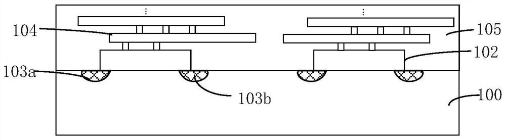
[0028] Figure 1~3 It is a structural schematic diagram corresponding to corresponding steps of a method for preparing a semiconductor device, such as figure 1 As shown, a substrate 100 is provided, and a plurality of gate structures 102 arranged in an array are formed on the substrate 100, and an active region 103a and a drain region 103b are formed in the substrate 100 on both sides of the gate structure 102; A first dielectric layer 105 is formed on the substrate 100, the first dielectric layer 105 covers the substrate 100 and the gate structure 102, and the first dielectric layer 105 has a plurality of stacked metal interconnections An interconnection layer 104, the metal interconnection layer 104 is electrically connected to at least one of the gate structure 102, the source region 103a or the drain region 103b.
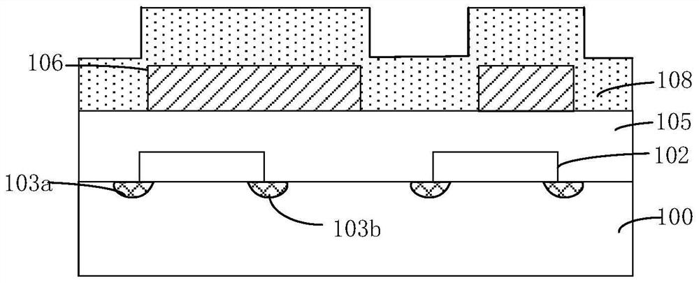
[0029] Such as figure 2 As shown, a patterned top metal layer 106 is formed on the first dielectric layer 105, and the top metal layer 106 communicates with ...
PUM
| Property | Measurement | Unit |
|---|---|---|
| Thickness | aaaaa | aaaaa |
Abstract
Description
Claims
Application Information