Ferroelectric field effect transistor memory device structure

A storage device and electric field effect technology, applied in the field of storage, can solve the problems of lack of anti-counterfeiting of label etching method, difficult to unify welding quality, uncontrollable deformation variable, etc., to improve the ability of anti-counterfeiting, strong installation stability, and enhanced anti-counterfeiting The effect of rust ability

Inactive Publication Date: 2022-04-29
HUNAN INSTITUTE OF ENGINEERING
View PDF0 Cites 0 Cited by
  • Summary
  • Abstract
  • Description
  • Claims
  • Application Information

AI Technical Summary

Problems solved by technology

[0003] The existing ferroelectric field effect transistor memory needs to etch a label on the surface of the shell during packaging, and the etching method is mostly laser engraving, but some merchants or private individuals will tamper with the etched label on the surface in order to seek greater benefits , in order to counterfeit more advanced chips for sale, the conventional label etching method lacks anti-counterfeiting, and cannot prevent this type of behavior. On the other hand, when soldering ferroelectric field effect transistor memories, there are many pins. The quality of welding directly affects the service life of the later period. The existing welding method will cause deformation to the welding plate of the pin, and the deformation cannot be controlled, so the welding quality is difficult to unify

Method used


Image

  • Ferroelectric field effect transistor memory device structure
  • Ferroelectric field effect transistor memory device structure
  • Ferroelectric field effect transistor memory device structure

Examples


Embodiment Construction

[0025] In order to make the technical means, creative features, goals and effects achieved by the present invention easy to understand, the present invention will be further described below in conjunction with specific embodiments.

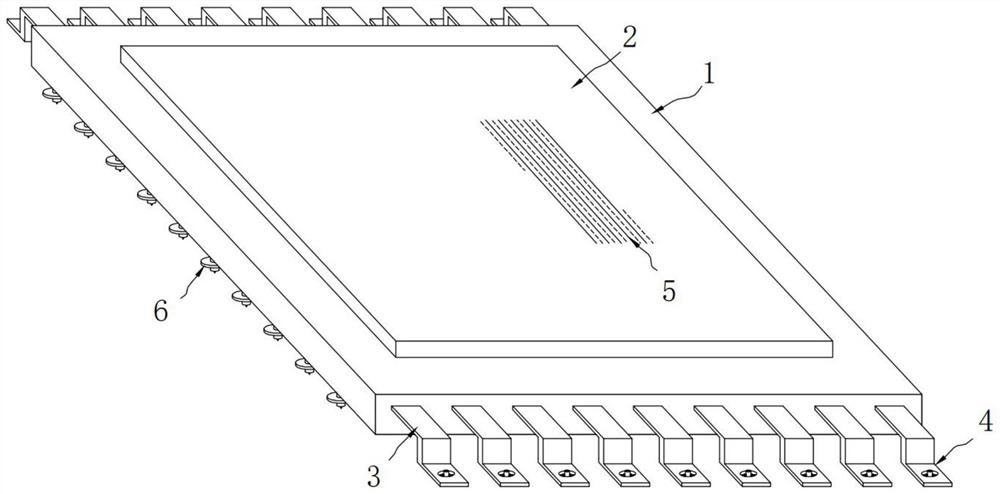
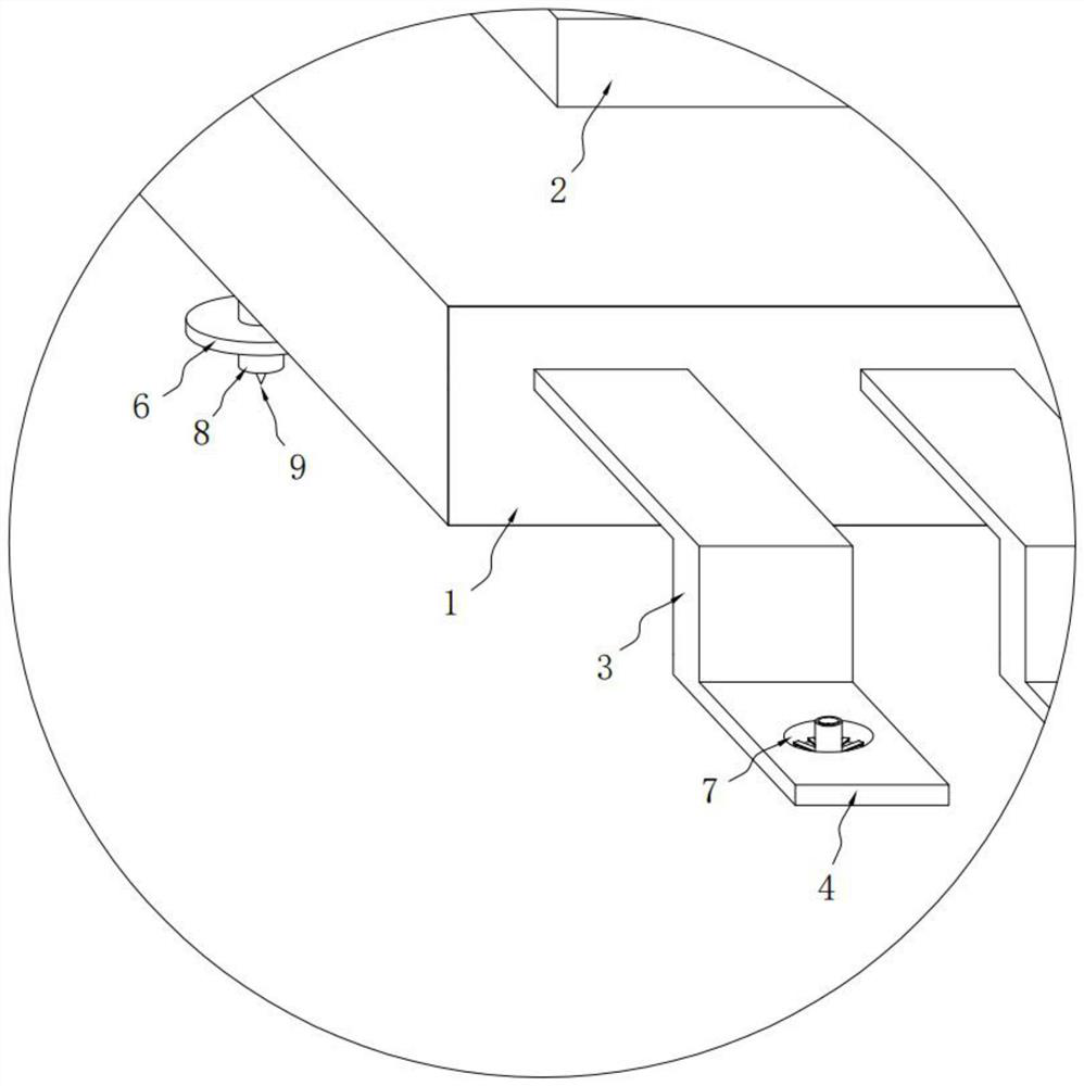
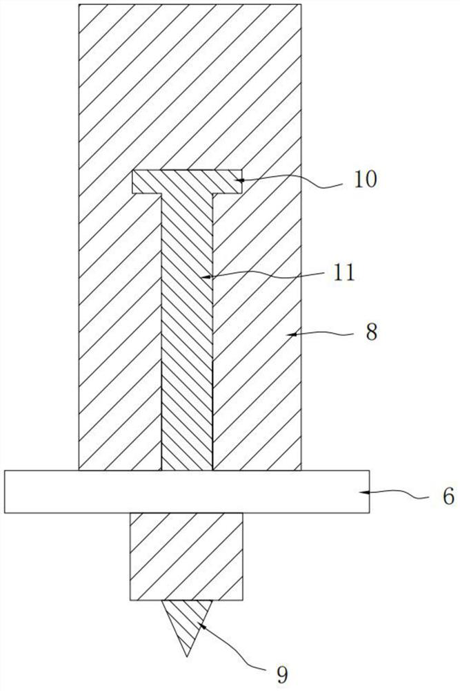
[0026] see Figure 1 to Figure 5 , the present invention provides a technical solution: a ferroelectric field effect transistor storage device structure, including a storage device structure body, the storage device structure body includes a shell 1, pins 3, a pressure plate 2 and a moisture-proof plate 6, the shell The surface of the body 1 is mounted with a pressure plate 2, the surface of the pressure plate 2 is provided with an information label 5, the inside of the housing 1 is provided with a protective layer 19, and the bottom end of the protective layer 19 is provided with a substrate 20, so The bottom end of the housing 1 is provided with an insulating column 8, and the bottom end of the insulating column 8 is mounted with a moisture-proo...


PUM


Abstract

A ferroelectric field effect transistor memory device structure provided by the present invention comprises a memory device structure body, the memory device structure body comprises a shell, pins, a pressing plate and a moisture-proof plate, the pressing plate is mounted on the surface of the shell, an information label is arranged on the surface of the pressing plate, a protection layer is arranged in the shell, and the moisture-proof plate is arranged in the shell. A substrate is arranged at the bottom end of the protective layer, an insulating column is arranged at the bottom end of the shell, a moisture-proof plate is attached to the bottom end of the insulating column, a plurality of pins are connected to the two sides of the shell, a welding plate is arranged at the tail ends of the pins, a tin column is arranged in the middle of the welding plate, and a copper bar is connected to the side edge of the tin column. The surface of the shell is coated with filling glue, the pressing plate is attached to the top of the shell through the filling glue, the ferroelectric field effect transistor storage device structure has efficient anti-fake and tamper-proof functions, welding is faster and more accurate, pin installation is more uniform and stable, and a certain moisture-proof effect is achieved.

Description

technical field [0001] The invention relates to the technical field of memory, in particular to a ferroelectric field effect transistor memory device structure. Background technique [0002] Ferroelectric field effect transistor memory has the advantages of high integration, fast read and write speed, low power consumption, and good compatibility with CMOS technology. Compared with ferroelectric random access memory with capacitor structure, its structure is simpler and higher integration ; Therefore, ferroelectric field effect transistor memory is widely considered to be one of the most potential memory in the next generation of memory. [0003] The existing ferroelectric field effect transistor memory needs to etch a label on the surface of the shell during packaging, and the etching method is mostly laser engraving, but some merchants or private individuals will tamper with the etched label on the surface in order to seek greater benefits , in order to counterfeit more a...

Claims


Application Information

Patent Timeline
Patent Type & Authority Applications(China)
IPC IPC(8): H01L23/057H01L23/544H01L23/00H05K1/18G11C11/40
CPCH01L23/057H01L23/564H01L23/544H05K1/181G11C11/40
Inventor 孙静龚希文谢斌贺聘彬苏焱鸿钟紫晴
Owner HUNAN INSTITUTE OF ENGINEERING
Why Eureka
Try Eureka