Repulsion mesh and deposition method

A deposition method and deposition process technology, used in coatings, gaseous chemical plating, discharge tubes, etc., can solve problems such as falling, particle contamination, affecting device quality, etc., and achieve the effect of reducing undercut and improving material interface density

Pending Publication Date: 2022-05-10
APPLIED MATERIALS INC
View PDF0 Cites 0 Cited by
  • Summary
  • Abstract
  • Description
  • Claims
  • Application Information

AI Technical Summary

Problems solved by technology

Particle contamination can become an increasing challenge as device dimensions continue to shrink
During the deposition process, material can be deposited on chamber components and this material can drop onto the substrate after deposition, which can affect device quality

Method used


Image

  • Repulsion mesh and deposition method
  • Repulsion mesh and deposition method
  • Repulsion mesh and deposition method

Examples


Embodiment Construction

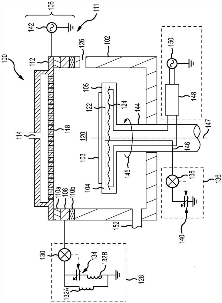
[0020] Plasma-enhanced deposition can generate a localized plasma between a showerhead or gas distributor and a substrate support during material deposition, such as material deposition of silicon oxide or other silicon-containing materials. When the precursor is activated in the plasma, deposition material can be formed and deposited on the substrate. While this deposition is occurring, additional deposition may also occur in the processing chamber, such as dead spaces within the chamber where fluid flow may not be ideal. Furthermore, the process of plasma generation may create a shell over the substrate that may circulate and trap certain particles. When the plasma is turned off, material attached to chamber components may flake off and fall onto the substrate, and particles previously trapped in the plasma may also fall onto the substrate. These additional particles can create defects in the deposited film, which can degrade or otherwise affect device quality.

[0021] Co...


PUM


Abstract

An exemplary deposition method may include electrostatically chucking a semiconductor substrate within a processing region of a semiconductor processing chamber at a first voltage. The method may include performing a deposition process. The deposition process may include forming a plasma within a processing region of a semiconductor processing chamber. The method may include stopping plasma formation within the semiconductor processing chamber. The method may include the step of increasing a first voltage of electrostatic chucking to a second voltage concurrently with the stopping step. The method may include purging a processing region of a semiconductor processing chamber.

Description

[0001] Cross References to Related Applications [0002] This application claims the benefit of priority to U.S. Provisional Patent Application No. 62 / 899,351, filed September 12, 2019, the contents of which are hereby incorporated in their entirety for all purposes. technical field [0003] This technology relates to semiconductor processing and chamber components. More specifically, the technology relates to modified components and deposition methods. Background technique [0004] Integrated circuits are made possible by processes that create intricately patterned layers of material on the surface of a substrate. Generating patterned materials on a substrate requires controlled methods of forming and removing exposed materials. Particle contamination can become an increasing challenge as device dimensions continue to shrink. During the deposition process, material may be deposited on chamber components, and this material may drop onto the substrate after deposition, whi...

Claims


Application Information

Patent Timeline
Patent Type & Authority Applications(China)
IPC IPC(8): H01L21/316H01L21/311H01L21/683C23C16/40C23C16/44H01J37/32
CPCH01L21/6833H01L21/02164H01L21/02274H01L21/31116H01J37/32715C23C16/401C23C16/4408H01L21/02216H01L21/02315H01J2237/3321H01J2237/334
Inventor M·S·K·穆蒂亚拉S·卡玛斯D·帕德希
Owner APPLIED MATERIALS INC
Why Eureka
Try Eureka