Array substrate, manufacturing method thereof and electronic paper display device
A technology of an array substrate and a manufacturing method, which is applied in the field of display devices, can solve problems such as abnormality and electronic ink crosstalk display, and achieve the effects of simple structure, good display effect, and good display effect
- Summary
- Abstract
- Description
- Claims
- Application Information
AI Technical Summary
Problems solved by technology
Method used
Image


Examples
Embodiment 1
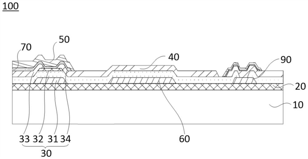
[0050] Please refer to figure 1 and figure 2 , Embodiment 1 of the first aspect of the present application proposes an array substrate 100 suitable for a dot-matrix electronic paper display device (Electronic Paper Display, EPD). The array substrate 100 includes a base substrate 10 , a first light shielding layer 20 , a thin film transistor 30 and a pixel electrode 40 .
[0051] The base substrate 10 can be a transparent substrate, such as a transparent glass substrate; in other embodiments, the base substrate 10 can also be a flexible substrate.
[0052] The first light-shielding layer 20 is disposed on the base substrate 10 , the first light-shielding layer 20 is opaque, and can prevent external light from entering from the side of the base substrate 10 and irradiating the thin film transistor 30 .
[0053]The thin film transistor 30 is disposed on the first light shielding layer 20 , that is, the thin film transistor 30 is disposed on a side of the first light shielding ...
Embodiment 2
[0066] Please refer to image 3 and Figure 4 Embodiment 2 of the first aspect of the present application proposes an array substrate 100, including a base substrate 10, a first light shielding layer 20 disposed on the base substrate 10, a thin film transistor 30 disposed on the first light shielding layer 20, and pixel electrode 40 .
[0067] The array substrate 100 provided in Embodiment 2 further includes a first insulating layer 70 , which is different from Embodiment 1 in that: the first insulating layer 70 and the pixel electrode 40 are sequentially stacked on the thin film transistor 30 , and the first insulating layer 70 is provided with There is an opening 71 ; the pixel electrode 40 is a conductive light-shielding material, and is electrically connected to the drain 34 through the opening 71 . The first insulating layer 70 functions as insulation and planarization.
[0068] Optionally, the pixel electrode 40 is made of metal or alloy, for example: AL (aluminum), A...
Embodiment 3
[0077] Please refer to Figure 5 and Figure 6 Embodiment 3 is similar to Embodiment 2. The array substrate 100 includes a base substrate 10, a first light shielding layer 20 disposed on the base substrate 10, a thin film transistor 30 disposed on the first light shielding layer 20, and a thin film transistor disposed on the base substrate 10. The first insulating layer 70 on the first insulating layer 70, and the pixel electrode 40 arranged on the first insulating layer 70, the pixel electrode 40 is a conductive light-shielding material, and is electrically connected to the drain electrode 34 through the opening 71 in the first insulating layer 70, The array substrate 100 has a relatively large aperture ratio.
[0078] Different from Embodiment 2, the array substrate 100 further includes a second light-shielding layer 50 disposed on the semiconductor layer 32 , and the second light-shielding layer 50 is on the same layer as the pixel electrodes 40 and arranged at intervals. ...
PUM
| Property | Measurement | Unit |
|---|---|---|
| reflectance | aaaaa | aaaaa |
Abstract
Description
Claims
Application Information
 - R&D
- Intellectual Property
- Life Sciences
- Materials
- Tech Scout
- Unparalleled Data Quality
- Higher Quality Content
- 60% Fewer Hallucinations
Browse by: Latest US Patents, China's latest patents, Technical Efficacy Thesaurus, Application Domain, Technology Topic, Popular Technical Reports.
© 2025 PatSnap. All rights reserved.Legal|Privacy policy|Modern Slavery Act Transparency Statement|Sitemap|About US| Contact US: help@patsnap.com