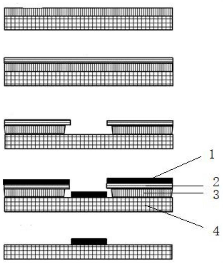
Preparation method of inverted trapezoidal photoresist side wall morphology and photoresist
A technology of photoresist and inverted trapezoid, which is applied in the direction of photosensitive material processing, semiconductor/solid-state device manufacturing, electrical components, etc., can solve the problems of increasing the difficulty of stripping, improve the quality of pattern transfer, make the method easy to operate, and improve chip integration Effect on Yield
- Summary
- Abstract
- Description
- Claims
- Application Information
AI Technical Summary
Problems solved by technology
Method used
Image
Examples
Embodiment 1
[0034] In this embodiment, the preparation method of the inverted trapezoidal photoresist sidewall morphology comprises the following steps:
[0035] (1) Pretreatment of the wafer: On the glue developer, pretreat the Si wafer with HMDS (hexamethyldisilazane) to enhance the surface adhesion, and then center it.
[0036] (2) Coating and pre-baking: Coat photoresist AZ6130 by spin coating with a thickness of 2.8um, then bake at 150°C for 60s, and then cool for 30s.
[0037] (3) Coating and pre-baking: Spin-coat another photoresist AZ703 with a thickness of 1.5um on the wafer that has been spin-coated with a layer of AZ6130 photoresist with a thickness of 2.8um.
[0038] (4) Exposure: set the exposure time to 430ms and the focus to -2.4um.
[0039] (5) Development: After optical exposure, the wafer is immersed in the developer solution, and developed for 60 seconds after the center is positioned to obtain a pattern.
[0040] (6) Hardening film: Harden the film at 120°C for 120s....
Embodiment 2
[0042] In this embodiment, the preparation method of the inverted trapezoidal photoresist sidewall morphology comprises the following steps:
[0043](1) Pretreatment of the wafer: On the glue developer, pretreat the Si wafer with trimethylsilyldiethylamine to enhance the surface adhesion, and then center it.
[0044] (2) Coating and pre-baking: Coat photoresist AZ6130 by spin coating with a thickness of 2.8um, then bake at 150°C for 60s, and then cool for 30s.
[0045] (3) Coating and pre-baking: Spin-coat another photoresist AZ703 with a thickness of 2.1 um on the wafer that has been spin-coated with a layer of AZ6130 photoresist with a thickness of 2.8 um.
[0046] (4) Exposure: set the exposure time to 500ms and the focus to -3.0um.
[0047] (5) Development: After optical exposure, the wafer is immersed in the developer solution, and developed for 60 seconds after the center is positioned to obtain a pattern.
[0048] (6) Hardening film: Harden the film at 120°C for 180s....
PUM
 Abstract
Description
Claims
Application Information
 - R&D
- Intellectual Property
- Life Sciences
- Materials
- Tech Scout
- Unparalleled Data Quality
- Higher Quality Content
- 60% Fewer Hallucinations
Browse by: Latest US Patents, China's latest patents, Technical Efficacy Thesaurus, Application Domain, Technology Topic, Popular Technical Reports.
© 2025 PatSnap. All rights reserved.Legal|Privacy policy|Modern Slavery Act Transparency Statement|Sitemap|About US| Contact US: help@patsnap.com

