Manufacturing method of SONOS (Silicon Oxide Nitride Oxide Semiconductor) device

A manufacturing method and device technology, applied in the fields of semiconductor/solid-state device manufacturing, semiconductor devices, electrical components, etc., can solve the problems of poor electronic capture capability of flash memory devices, poor device performance, unstable process, etc., and increase retention time. , the effect of increasing the proportion and improving the reliability

Pending Publication Date: 2022-05-24
SHANGHAI HUALI INTEGRATED CIRCUTE MFG CO LTD
View PDF0 Cites 0 Cited by
  • Summary
  • Abstract
  • Description
  • Claims
  • Application Information

AI Technical Summary

Problems solved by technology

[0004] In view of the shortcomings of the prior art described above, the purpose of the present invention is to provide a method for manufacturing a SONOS device, which is used to solve the problems of poor electron capture ability of flash memory devices in the prior art, instability in the process, and poor device performance.

Method used


Image

  • Manufacturing method of SONOS (Silicon Oxide Nitride Oxide Semiconductor) device
  • Manufacturing method of SONOS (Silicon Oxide Nitride Oxide Semiconductor) device

Examples


Embodiment 1

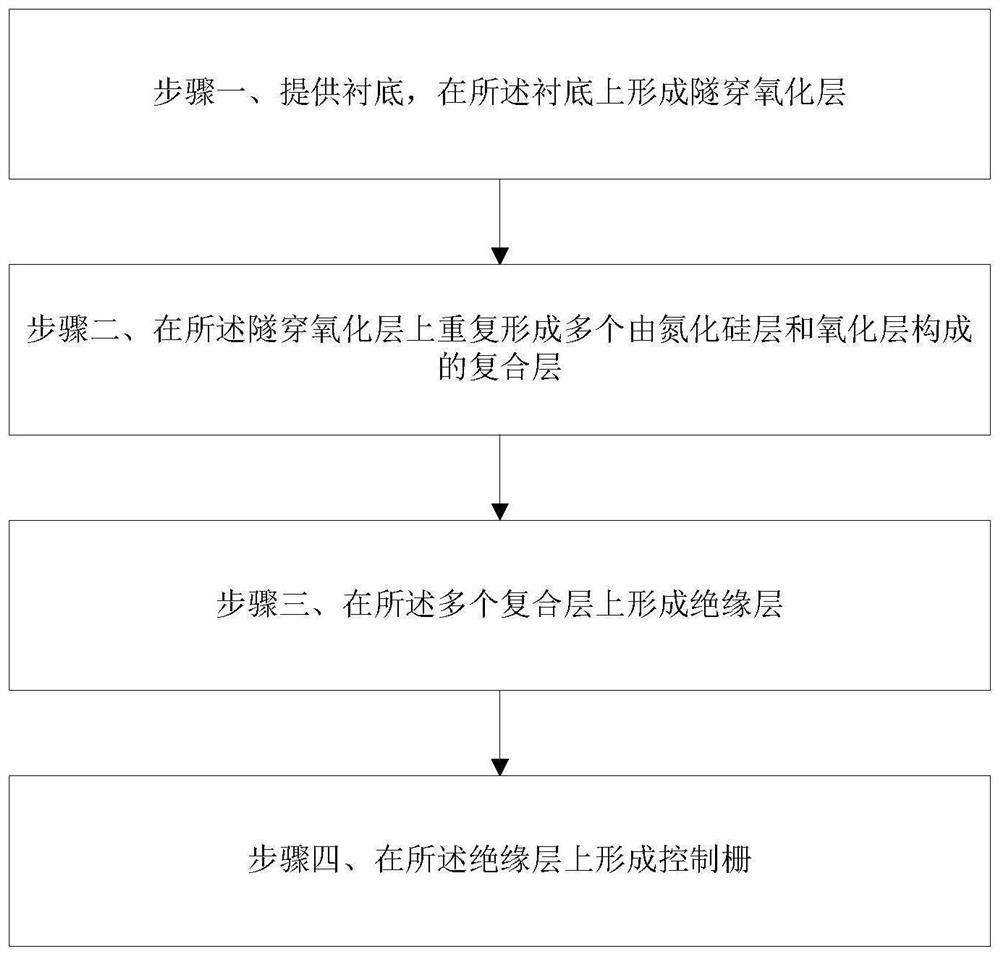
[0024] The invention provides a manufacturing method of a SONOS device, such as figure 2 shown, figure 2 Shown is the flow chart of the manufacturing method of the SONOS device of the present invention, and the method at least comprises the following steps:

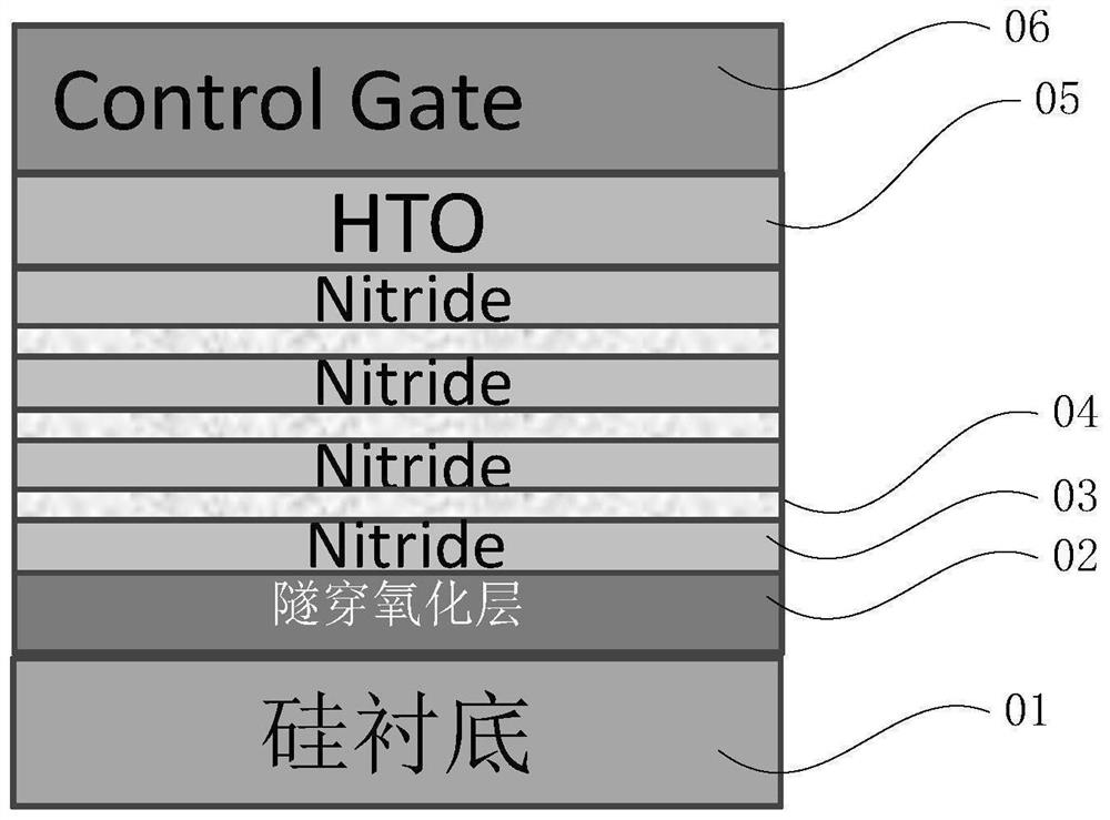
[0025] Step 1, providing a substrate, and forming a tunnel oxide layer on the substrate; such as figure 1 shown, figure 1 Shown is a schematic structural diagram of forming a tunnel oxide layer, a composite layer, an insulating layer and a control gate on a substrate in the present invention. In step 1, a tunnel oxide layer 02 is formed on the substrate 01 .

[0026] Further, in the present invention, the substrate 01 in step 1 of this embodiment is a silicon substrate, an active region is provided on the silicon substrate, and the tunnel oxide layer 02 is formed on the silicon substrate of the active region.

[0027] Step 2: Repeatedly forming a plurality of composite layers consisting of a silicon nitride layer a...

Embodiment 2

[0037] The invention provides a manufacturing method of a SONOS device, such as figure 2 shown, figure 2 Shown is the flow chart of the manufacturing method of the SONOS device of the present invention, and the method at least comprises the following steps:

[0038] Step 1, providing a substrate, and forming a tunnel oxide layer on the substrate; such as figure 1 shown, figure 1 Shown is a schematic structural diagram of forming a tunnel oxide layer, a composite layer, an insulating layer and a control gate on a substrate in the present invention. In step 1, a tunnel oxide layer 02 is formed on the substrate 01 .

[0039] Further, in the present invention, the substrate 01 in step 1 of this embodiment is a silicon substrate, an active region is provided on the silicon substrate, and the tunnel oxide layer 02 is formed on the silicon substrate of the active region.

[0040] Step 2: Repeatedly forming a plurality of composite layers consisting of a silicon nitride layer a...


PUM


Abstract

The invention provides a manufacturing method of an SONOS device, and the method comprises the steps: providing a substrate, and forming a tunneling oxide layer on the substrate; repeatedly forming a plurality of composite layers consisting of silicon nitride layers and oxide layers on the tunneling oxide layer; forming an insulating layer on the plurality of composite layers; and forming a control gate on the insulating layer. The multi-level trap energy level is manufactured by manufacturing the multiple silicon nitride trap layers, the proportion of the deep trap energy level can be improved, the retention time of electric charges limited in deep traps is prolonged, and therefore the reliability of the device is improved.

Description

technical field [0001] The invention relates to the technical field of semiconductors, in particular to a method for manufacturing a SONOS device. Background technique [0002] The traditional SONOS (flash memory) device process is to first deposit a tunnel oxide layer on the silicon substrate, then deposit a layer of silicon nitride for trapping electrons, and finally a layer of insulating layer and growth of polysilicon control gate. [0003] The traditional SONOS process uses the defects of the silicon nitride trap layer to realize programming and erasing operations under the action of a high electric field, which is suitable for consumer electronic memory modules, but with high temperature scenarios, the shallow energy level traps in silicon nitride decay. It is very obvious, so it is particularly urgent to be able to design more deep-level traps. SUMMARY OF THE INVENTION [0004] In view of the above-mentioned shortcomings of the prior art, the purpose of the present...

Claims


Application Information

Patent Timeline
Patent Type & Authority Applications(China)
IPC IPC(8): H01L21/336H01L21/28H01L29/792
CPCH01L29/66833H01L29/40117H01L29/792
Inventor 钱亚峰熊凌昊黄冠群
Owner SHANGHAI HUALI INTEGRATED CIRCUTE MFG CO LTD
Why Eureka
Try Eureka