Wafer-level electric leakage reducing ESD structure

A wafer-level, resistive technology, applied to circuits, emergency protection circuit devices for limiting overcurrent/overvoltage, transistors, etc. problems, to achieve the effect of suppressing sub-threshold current, ensuring ESD performance, and reducing circuit power consumption

Pending Publication Date: 2022-06-07
中国人民解放军96901部队23分队
View PDF5 Cites 0 Cited by
  • Summary
  • Abstract
  • Description
  • Claims
  • Application Information

AI Technical Summary

Problems solved by technology

[0004] In the prior art, for the leakage protection between the power supply of the transmitting end and the power supply of the receiving end, at present, the termination resistance and the current source are mainly closed. Even if the leakage path of the driver stage itself is turned off, due to the ESD on the IO interface Diode, when the power supply of the sending end drops to the conduction voltage of the diode, the ESD diode will still conduct, and there will still be a leakage path, which cannot completely cut off the leakage current path, resulting in unnecessary leakage power consumption and reducing the IO chip service life

Method used


Image

  • Wafer-level electric leakage reducing ESD structure
  • Wafer-level electric leakage reducing ESD structure
  • Wafer-level electric leakage reducing ESD structure

Examples


Embodiment Construction

[0027] In order to further illustrate the various embodiments, the present invention provides accompanying drawings, which are part of the disclosure of the present invention, and are mainly used to illustrate the embodiments, and can be used in conjunction with the relevant descriptions in the specification to explain the operation principles of the embodiments. For these, those of ordinary skill in the art will understand other possible implementations and the advantages of the present invention. Components in the figures are not drawn to scale, and similar component symbols are generally used to represent similar components.

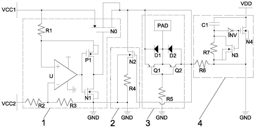
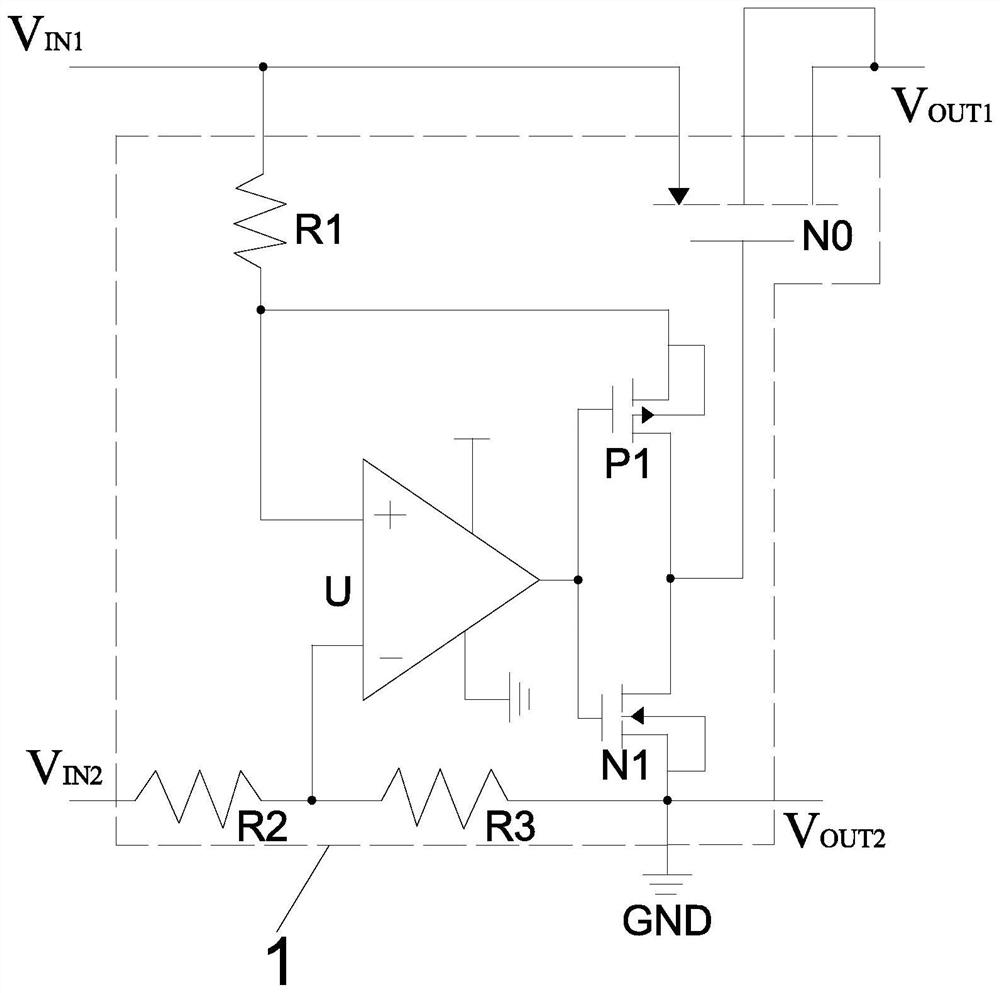
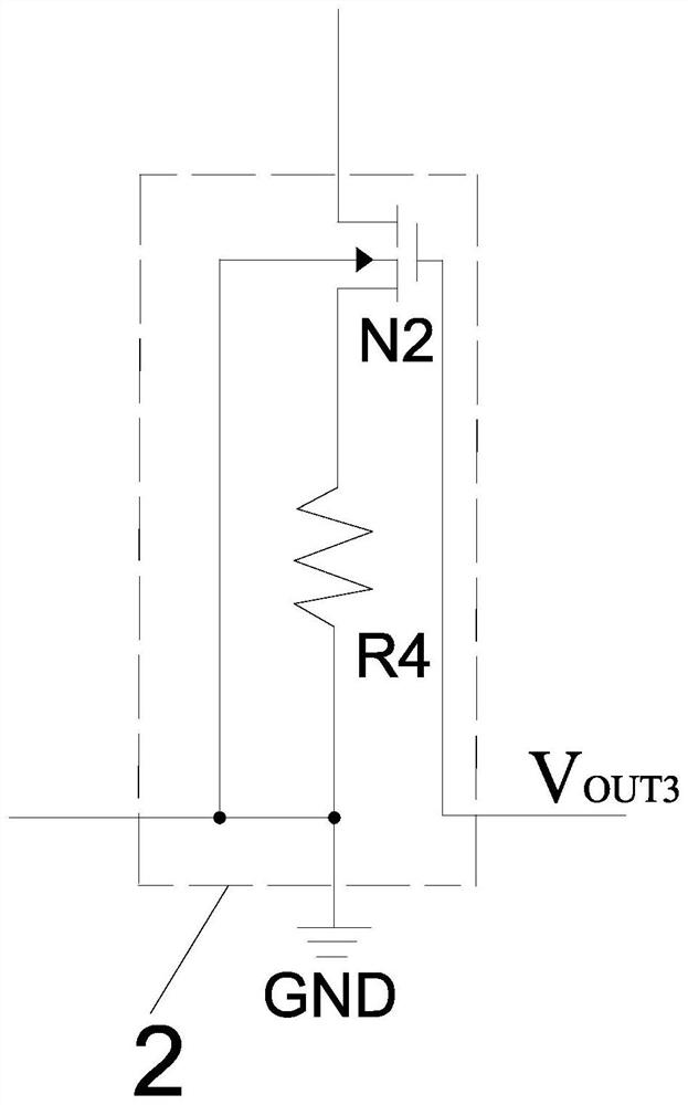
[0028] According to an embodiment of the present invention, an ESD structure with reduced leakage at the wafer level is provided.

[0029] The present invention will now be further described with reference to the accompanying drawings and specific embodiments, such as Figure 1-Figure 5 As shown, the wafer-level ESD structure for reducing leakage acco...


PUM


Abstract

The invention discloses a wafer-level electric leakage reducing ESD (Electro-Static Discharge) structure, which comprises a control circuit, a feedback circuit, a bleeder circuit and a clamping circuit which are packaged by adopting a wafer-level packaging process, wherein the first input end of the control circuit is connected with a power supply VCC1, the second input end of the control circuit is connected with a power supply VCC2, the first output end of the control circuit is sequentially connected with the feedback circuit, the bleeder circuit and the clamping circuit, and the second output end of the control circuit is connected with the feedback circuit; the output end of the feedback circuit is connected with the output end of the bleeder circuit; the output end of the bleeder circuit is connected with the first input end of the clamping circuit, and the second input end of the clamping circuit is connected with a power supply VDD. Through the control circuit, the feedback circuit, the bleeder circuit and the clamping circuit which are packaged by a wafer-level process, the occupied area of a chip can be effectively reduced, the stability of output voltage is improved, the safety and stability of the chip and the circuit after ESD (Electro-Static Discharge) occur are ensured, and meanwhile, the loss caused by electric leakage is reduced.

Description

technical field [0001] The present invention relates to the field of electrostatic protection circuits, in particular, to an ESD structure for reducing leakage current at the wafer level. Background technique [0002] Electrostatic discharge (ESD (Electro-Static discharge)) is a common phenomenon in nature. And static electricity is a deadly threat to integrated circuit chips. It can generate a large current in a short period of time and cause irreversible damage to integrated circuit chips. According to statistics, the economic loss caused by electrostatic discharge in the semiconductor manufacturing industry reaches billions of dollars every year. Therefore, ESD protection design has also become an indispensable link in integrated circuit design. However, there is also an irreconcilable contradiction between the anti-ESD capability of the integrated circuit chip itself and the development direction of the integrated circuit. The design purpose of the ESD protection circ...

Claims


Application Information

Patent Timeline
Patent Type & Authority Applications(China)
IPC IPC(8): H02H9/04H02H7/20H01L27/02
CPCH02H9/04H02H9/045H02H7/205H01L27/0266H01L27/0288H01L27/0255H01L27/0259
Inventor 程金星王庆波于艾温伟伟吴友朋
Owner 中国人民解放军96901部队23分队
Why Eureka
Try Eureka