
Optical Gyro Integrated Chip Based on Silicon Carbide Photonic Integration Platform on Insulator Substrate

A photonic integration technology on an insulating substrate, applied in the field of integrated optics and inertial sensing, can solve the problems of large waveguide loss, inability to epitaxial growth, interface defects, etc., achieve a large scale factor, suppress temperature drift effects, and improve stability. sexual effect

Active Publication Date: 2022-08-02
SHENZHEN OSNAV IND CO LTD
View PDF8 Cites 0 Cited by
  • Summary
  • Abstract
  • Description
  • Claims
  • Application Information

AI Technical Summary

Problems solved by technology

Due to the lattice constant mismatch with Si, there are interface defects in the 3C-SiC film grown directly on the silicon surface by heteroepitaxy, resulting in large waveguide loss; while the temperature required for 4H-SiC epitaxy is higher than the melting temperature of the silicon substrate , cannot be directly epitaxially grown on silicon substrates

Method used


Image

  • Optical Gyro Integrated Chip Based on Silicon Carbide Photonic Integration Platform on Insulator Substrate
  • Optical Gyro Integrated Chip Based on Silicon Carbide Photonic Integration Platform on Insulator Substrate
  • Optical Gyro Integrated Chip Based on Silicon Carbide Photonic Integration Platform on Insulator Substrate

Examples


Embodiment approach

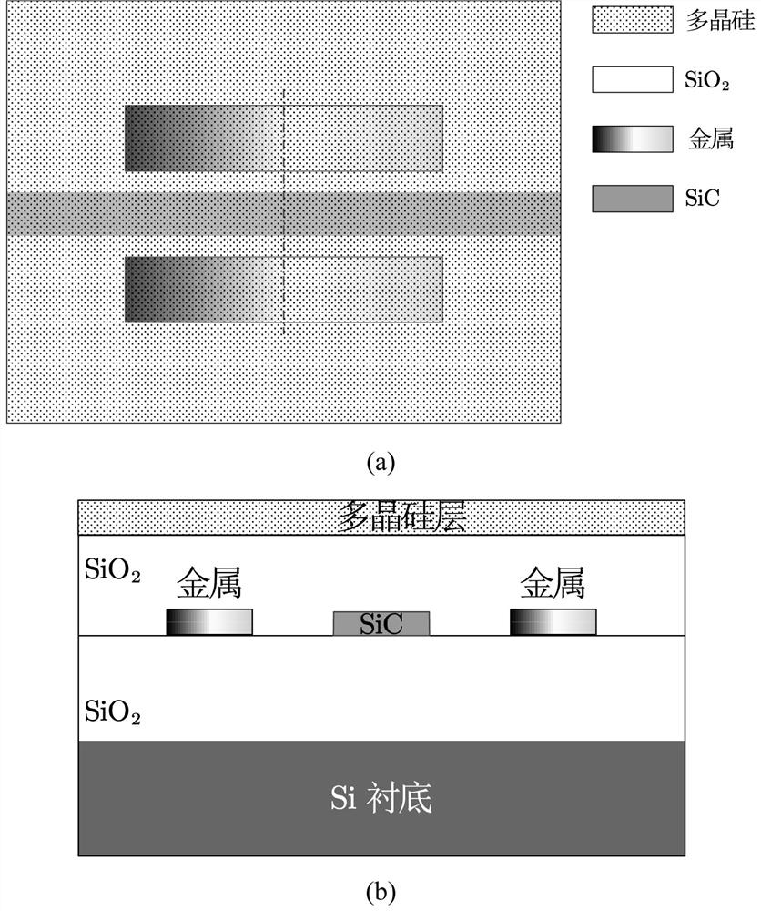
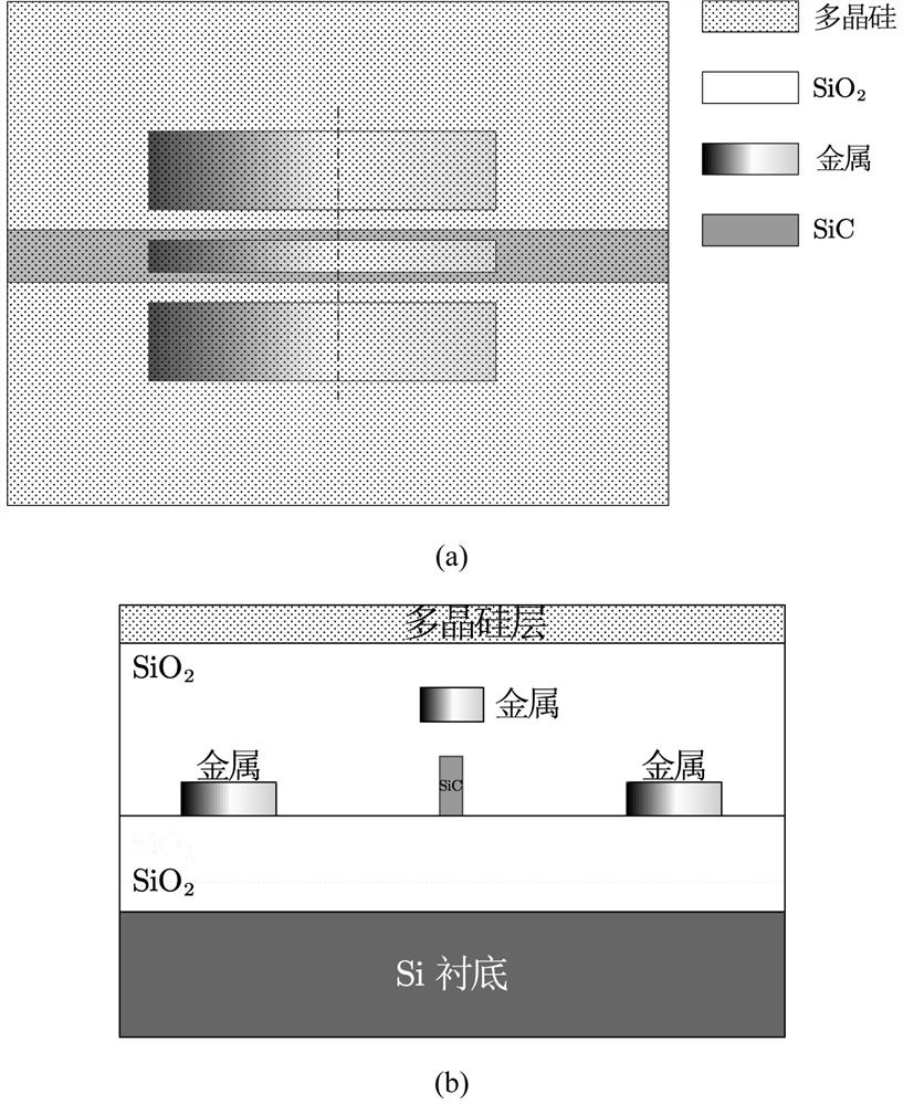
[0039] The phase shifter of the present invention can realize phase modulation by utilizing the linear electro-optic effect of SiC material, and its maximum electro-optic coefficient component d 33 About 32~38pm / V, according to the orientation of the crystal axis [0,0,1] of the SiC crystal, the phase shifter electrode structure can be designed horizontally or vertically. As an embodiment, the first phase shifter and the second phase shifter are designed with a horizontal electrode structure, that is, the corresponding crystal axis [0,0,1] is parallel to the chip plane, and the phase shifter structure design is as follows Figure 4 shown, from top to bottom: polysilicon layer, SiO 2 Overcladding, metal electrodes and SiC waveguides, SiO 2 Buried layer, Si substrate. The distribution of the RF electric field in the SiC waveguide is mainly along the horizontal direction, which can increase the RF electric field and the quasi-TE of the waveguide. 0 Overlap factor between optica...


PUM

PropertyMeasurementUnit
diameteraaaaaaaaaa
Mohs hardnessaaaaaaaaaa

Abstract

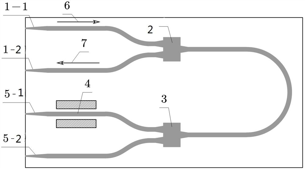
The embodiment of the present invention discloses an optical gyro integrated chip based on a silicon carbide photonics integration platform on an insulating substrate, comprising a first fiber-SiC waveguide coupler, a second fiber-SiC waveguide coupler, a first 3dB beam splitter, The second 3dB splitter, the first phase shifter, the second phase shifter, the third fiber-SiC waveguide coupler, the fourth fiber-SiC waveguide coupler; the difference between the first and second fiber-SiC waveguide couplers Connect to two branches of the first 3dB beam splitter; the first 3dB beam splitter is connected to the fundamental waveguide of the second 3dB beam splitter; one branch of the second 3dB beam splitter is connected to the third fiber through the first phase shifter ‑SiC waveguide coupler, and the other branch connects to the fourth fiber ‑SiC waveguide coupler. The invention can effectively improve the stability and reliability of the fiber optic gyroscope while ensuring the accuracy of the fiber optic gyroscope, improve the multiple performances of the fiber optic gyroscope, and realize the smaller size, lower power consumption, lower cost, simpler structure design and craft.

Description

technical field [0001] The invention relates to the technical field of integrated optics and inertial sensing, in particular to an optical gyro integrated chip based on a silicon carbide photonics integrated platform on an insulating substrate. Background technique [0002] Because it can achieve high-precision and high-reliability positioning, attitude control and absolute direction measurement, fiber-optic gyroscopes are widely used in space technology, military applications, and many civil fields such as car navigation and robotics. Fiber optic gyroscopes generally realize the generation, modulation and detection of optical signals based on separate fiber optic devices. Different fiber optic devices are spliced ​​by pigtails to form Sagnac interference optical circuits, which inevitably generate parasitic reflections at the connection point, additional insertion loss and pairing. The external environment is sensitive to polarization mismatch and other problems, which in t...

Claims


Application Information

Patent Timeline
Patent Type & Authority Patents(China)
IPC IPC(8): G01C19/72
CPCG01C19/722G01C19/725
Inventor 刘晓平吕海斌
Owner SHENZHEN OSNAV IND CO LTD
Learn More