Manufacturing method of outer-layer thin circuit of flexible circuit board

A technology for flexible circuit boards and manufacturing methods, which is applied in the fields of printed circuit manufacturing, removal of conductive materials by chemical/electrolytic methods, printed circuits, etc., which can solve the problems that dry films cannot meet the requirements of flexible circuit board manufacturing processes, etc., and achieve increased filling and the ability to cover holes and the effect of thickening the thickness

Pending Publication Date: 2022-06-17
MFLEX YANCHENG CO LTD
View PDF0 Cites 0 Cited by
  • Summary
  • Abstract
  • Description
  • Claims
  • Application Information

AI Technical Summary

Problems solved by technology

[0004] In view of this, the embodiment of the present invention provides a method for manufacturing thin lines on the outer layer of a flexible circuit board, so as to solve the problem that the dry film of the prior art cannot meet the requirements of the current flexible circuit board manufacturing process

Method used


Image

  • Manufacturing method of outer-layer thin circuit of flexible circuit board
  • Manufacturing method of outer-layer thin circuit of flexible circuit board
  • Manufacturing method of outer-layer thin circuit of flexible circuit board

Examples


example 1

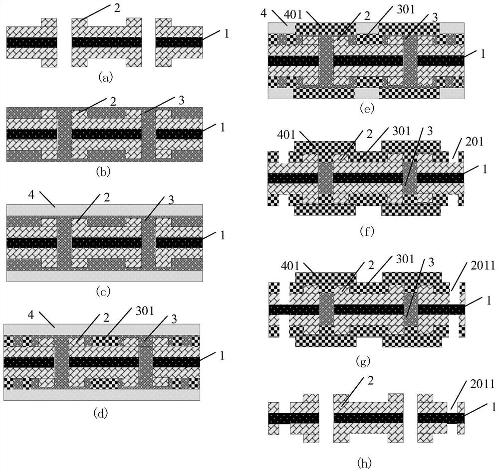
[0045] like figure 1 As shown, two types of dry films with different photosensitive wavelengths were selected to achieve differential curing. The first layer is a high-sensitivity LDI high-resolution, high-adhesion dry film with a 405nm light source. Then choose ordinary UV dry film (non-LDI dry film) with weak or no absorption at 405nm light source. The first step is to use a 405nm light source to perform pattern exposure except for the through-hole area. Because the upper layer of dry film has almost no absorption of 405nm light waves, the light waves reach the lower layer of dry film, that is, the curing of the bottom layer of dry film is completed, and the difference between the two layers of dry film is realized. cured. The second step uses a 355nm (or 375nm) light source to implement only the through-hole area curing, while controlling the degree of reaction of the deep dry film in the hole.

[0046] like figure 1 As shown in (a), a double-sided board is drilled, the...

example 2

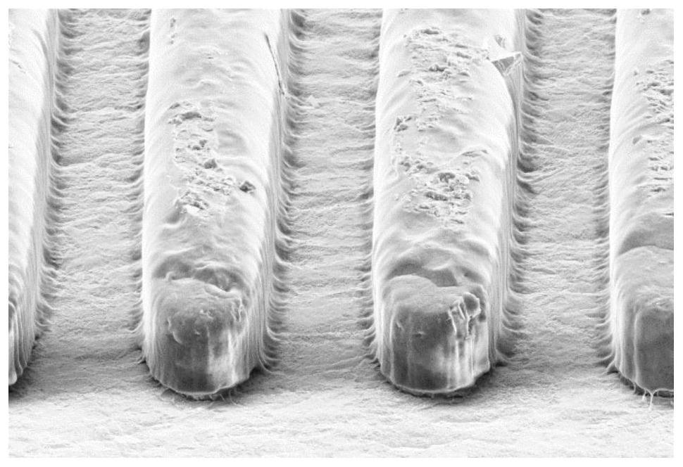
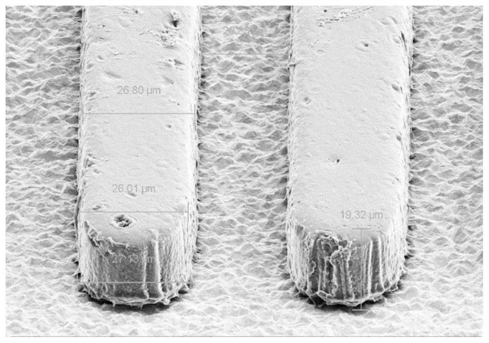
[0056] 1. The first layer is a dry film of LDI with high resolution, high adhesion, and not limited to laser light sources. First, use a 355nm (or 375nm) or 405nm or mixed wavelength laser light source for exposure outside the through-hole area, tear off the surface PET, and then paste a second layer of dry film. In order to improve the exposure efficiency, ordinary dry film UV dry film or LDI dry film can be used for the second layer of dry film. In order to improve the efficiency, LDI dry film is preferred, and a dry film with strong absorption of 355nm or 375nm wavelength laser is selected for through-hole area exposure. Realize the curing of the through-hole area, enhance the porosity, and at the same time control the reaction degree of the deep dry film in the hole, and it is easy to complete the film removal.

[0057] 2. Since the second exposure is only for the through hole area, during development, the dry film outside the upper through hole area will be revealed by th...


PUM


Abstract

The invention discloses a manufacturing method of an outer-layer thin circuit of a flexible circuit board. The manufacturing method comprises the following steps: laminating at least two layers of dry films on the surface of an outer-layer circuit board; the two layers of dry films are an inner-layer dry film and an outer-layer dry film of which the exposure patterns are not completely overlapped; developing the dry film which is not exposed; etching the exposed metal layer on the outer circuit board; removing the dry film; wherein the inner-layer dry film is locally exposed at positions except for the through holes and the blind holes on the outer-layer circuit board; the outer layer dry film and the inner layer dry film are exposed at the positions corresponding to the through holes and the blind holes in the outer layer circuit board at the same time, so that the inner layer dry film and the outer layer dry film form differential exposure and curing in the circuit pattern area. The double-layer dry film is overlaid, the thickness is increased, the filling and hole covering capacity is improved, meanwhile, the reaction degree of the deep dry film in the hole is controlled, and film removal is easy to complete.

Description

technical field [0001] The invention relates to the technical field of circuit board manufacturing, in particular to a method for manufacturing thin lines on the outer layer of a flexible circuit board. Background technique [0002] Flexible Printed Circuit Board (FPC) uses a key material called photosensitive dry film, also called photoresist, when making circuits. At present, according to the different models used, it is divided into ordinary UV dry film and LDI dry film. Ordinary UV dry film can be used for high pressure mercury light source and LED light source, LDI dry film is used for laser light source, there are three wavelengths, 355nm, 405nm, 375nm&405nm mixed wave. Among them, the 375nm&405nm mixed-wave LDI exposure machine can adjust the ratio of the two wavelengths, and a single wavelength can be from 0% to 100%. Because the difference between 375nm and 355nm on the photosensitive dry film is small, the two are usually not distinguished. In the production pro...

Claims


Application Information

Patent Timeline
Patent Type & Authority Applications(China)
IPC IPC(8): H05K3/06
CPCH05K3/061
Inventor 冯志强胡宗敏
Owner MFLEX YANCHENG CO LTD
Why Eureka
Try Eureka