Chip test probe and chip test device
A technology of chip testing and testing probes, which is applied in the direction of measuring devices, electronic circuit testing, measuring electricity, etc., can solve the problems of error, testing electric shock, increasing the difficulty of testing, and inaccurate testing data, so as to reduce the number of probes and measure The effect of rich data and high measurement accuracy
Inactive Publication Date: 2022-06-21
STELIGHT INSTR CO LTD
View PDF10 Cites 1 Cited by
- Summary
- Abstract
- Description
- Claims
- Application Information
AI Technical Summary
Problems solved by technology
[0004] However, in the process of testing through the thermistor, the thermistor needs to be powered on. This process itself will bring additional heat and increase the chip temperature, which will lead to inaccurate test data, and the indirect thermistor The way of testing the chip temperature is also the cause of the error
In addition, in order to increase the location and test points of the bonding thermistor, it is necessary to change the packaging method of the chip, so the chip size cannot be made smaller, and the increased test electric shock (that is, the thermistor and its corresponding test probe) also increases. Difficulty of the test
Method used
View moreImage
Smart ImageViewing Examples

Examples
Embodiment Construction
Login to View More PUM
 Abstract
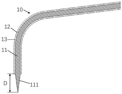
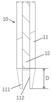
The invention provides a chip testing probe and a chip testing device, and belongs to the technical field of chip testing. The chip test probe comprises a test probe body used for detecting an electric signal on a to-be-tested chip when a test end portion of the test probe body is in contact with the to-be-tested chip; the light guide part is made of high-purity silicon dioxide and used for conducting light signals, the light guide part is arranged on the peripheral side surface of the test probe body or in the test probe body, one end of the light guide part is used for being arranged opposite to the chip to be tested, and the other end of the light guide part is used for being connected with an infrared temperature measuring device. And the infrared temperature measuring device calculates the temperature of the chip to be measured according to the received optical signal which is emitted by the chip to be measured and is conducted through the light guide part. According to the chip test probe and the chip test device, the measurement accuracy of the chip temperature can be improved.
Description
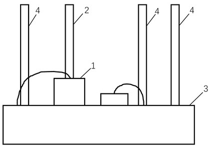
Technical field [0001] The invention involves the field of chip testing technology, especially a chip test probe and chip testing device. Background technique [0002] In the process of converting electrical energy into light energy, a large part of the electrical energy is converted into unnecessary thermal energy. The thermal energy will affect the performance and life of the laser chip. Therefore, the laser chip needs to be tested.Filtering chips with performance. [0003] like figure 1 It is shown that the existing technology generally increases thermal resistance on the laser chip 3 to predict the temperature of the laser chip 3 by measuring the resistance value of the thermistor.This scheme needs to add the corresponding test probe 2 to the testing tool to read the information of the thermistor 1.When testing the electrical signal, you still need to test the probe 4. [0004] However, in the process of testing through the thermal resistance, the heat -sensitive resistance i...
Claims
Login to View More Application Information
Patent Timeline
 Patent Type & Authority Applications(China)
IPC IPC(8): G01R1/073G01R31/28G01J5/00
CPCG01R1/073G01R31/282G01J5/0096
Inventor 罗跃浩黄建军胡海洋
Owner STELIGHT INSTR CO LTD
Features
- R&D
- Intellectual Property
- Life Sciences
- Materials
- Tech Scout
- Unparalleled Data Quality
- Higher Quality Content
- 60% Fewer Hallucinations
Learn More Browse by: Latest US Patents, China's latest patents, Technical Efficacy Thesaurus, Application Domain, Technology Topic, Popular Technical Reports.
© 2025 PatSnap. All rights reserved.Legal|Privacy policy|Modern Slavery Act Transparency Statement|Sitemap|About US| Contact US: help@patsnap.com