

Planar power semiconductor device
A technology for power semiconductors and devices, applied in the field of planar power semiconductor devices, can solve the problem that wide bandgap semiconductors cannot be applied, and achieve the effects of reducing energy loss, reducing specific on-resistance, and simplifying process flow
- Summary
- Abstract
- Description
- Claims
- Application Information
AI Technical Summary
Problems solved by technology
Method used
Image

Examples
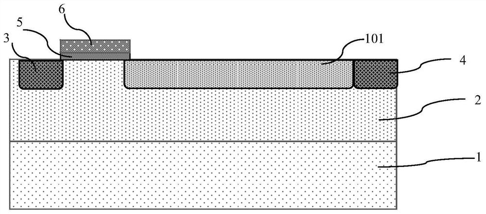
no. 1 example
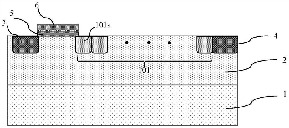
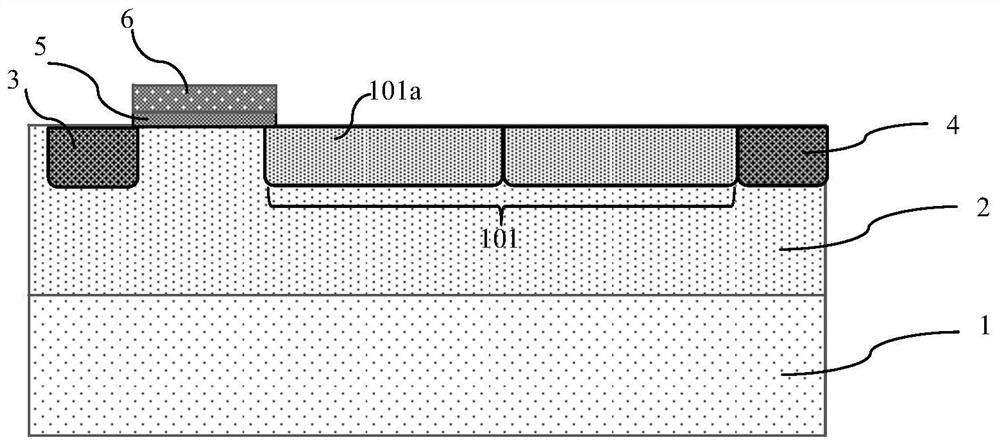
[0083] like figure 2 As shown, it is a schematic structural diagram of the planar power semiconductor device according to the second embodiment of the present invention; compared with the first embodiment of the present invention, the planar power semiconductor device according to the second embodiment of the present invention has the following features:
[0084] Under the condition that the total doping dose of the drift region 101 is kept unchanged, the drift region 101 is divided into a plurality of drift sub-regions 101a in the lateral direction, and the doping concentration of each drift sub-region 101a is different The setting of the doping concentration of the drift sub-region 101a regulates and regulates the surface electric field of the drift region 101 to make the surface electric field distribution of the drift region 101 uniform. figure 2 , each of the drift sub-regions is individually marked with a mark 101a.
[0085] The widths of the drift sub-regions 101a ar...
PUM
 Abstract
Description
Claims
Application Information