
PCB surface defect detection method based on frequency domain information double confirmation

A technology of defect detection and frequency domain, applied in image analysis, image enhancement, instruments, etc., can solve problems such as limiting PCB supply quality and imaging noise interference, and achieve improved PCB supply quality, high robustness, and fast evaluation speed Effect

Inactive Publication Date: 2022-06-24
爱科赛智能科技(浙江)有限公司
View PDF18 Cites 0 Cited by
  • Summary
  • Abstract
  • Description
  • Claims
  • Application Information

AI Technical Summary

Problems solved by technology

Up to now, most inspection systems on the production line are based on edge detection algorithms for quality inspection, but edge detection methods are susceptible to imaging noise interference, which limits the further improvement of PCB supply quality

Method used


Image

  • PCB surface defect detection method based on frequency domain information double confirmation
  • PCB surface defect detection method based on frequency domain information double confirmation
  • PCB surface defect detection method based on frequency domain information double confirmation

Examples


Embodiment 1

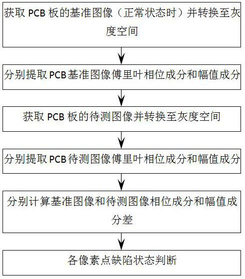
[0051] Embodiment 1: A PCB surface defect detection method based on double confirmation of frequency domain information, the flowchart of which is as follows: figure 1 As shown, establishing a PCB image acquisition device also includes the following steps:

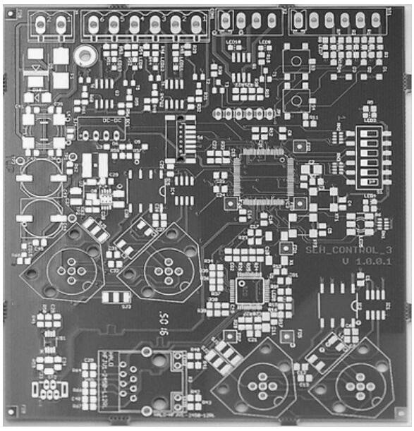
[0052] S1: Obtain the reference image of the PCB board to obtain the PCB reference image (in normal state), and convert it to gray space; figure 2 The specific conversion method is as follows:

[0053]

[0054] Among them, I is the generated grayscale image, R is the red channel of the color image, G is the green channel of the color image, and B is the blue channel of the color image

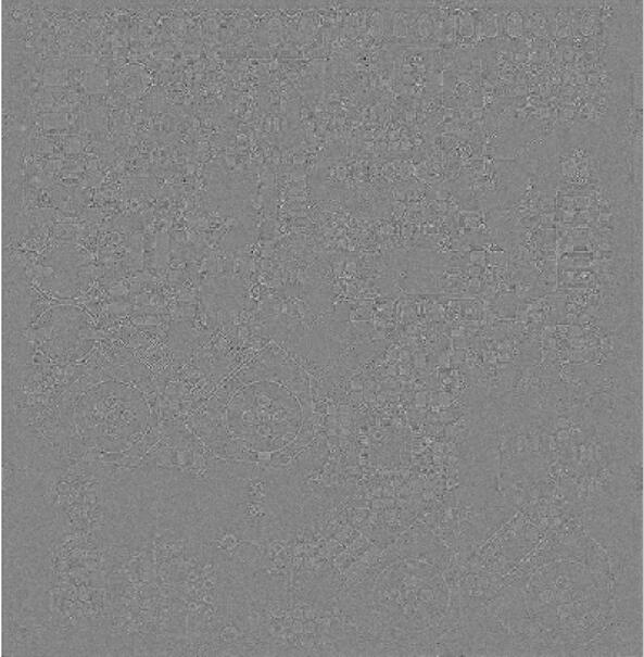
[0055] S2: Extract the Fourier phase component and amplitude component of the PCB reference image respectively; image 3 , attached Figure 4As shown, the extraction method of the Fourier phase component and the amplitude component of the image includes the following steps:

[0056] SS1: Calculate the two-dimensional Fourier transfo...

Embodiment 2

[0072] Embodiment 2: A PCB surface defect detection method based on double confirmation of frequency domain information, the flowchart of which is as follows: figure 1 As shown, establishing a PCB image acquisition device also includes the following steps:

[0073] S1: Obtain the reference image of the PCB board to obtain the PCB reference image (in normal state), and convert it to gray space; Figure 12 The specific conversion method is as follows:

[0074]

[0075] Among them, I is the generated grayscale image, R is the red channel of the color image, G is the green channel of the color image, and B is the blue channel of the color image

[0076] S2: Extract the Fourier phase component and amplitude component of the PCB reference image respectively; Figure 13 , attached Figure 14 As shown, the extraction method of the Fourier phase component and the amplitude component of the image includes the following steps:

[0077] SS1: Calculate the two-dimensional Fourier tr...


PUM


Abstract

The invention discloses a PCB (Printed Circuit Board) surface defect detection method based on frequency domain information double confirmation. The method comprises the following steps: firstly, acquiring a reference image (in a normal state) of a PCB and converting the reference image into a gray scale space; respectively extracting a Fourier phase component and an amplitude component of the PCB reference image; obtaining a to-be-detected image of the PCB and converting the to-be-detected image to a gray scale space Fourier phase components and amplitude components of the to-be-detected image of the PCB are extracted respectively; respectively calculating phase component and amplitude component differences of the normalized reference image and the image to be measured; and if the phase component difference and the amplitude component difference of the same position are both greater than a preset threshold, determining that the position has defects. The method has the advantages of high evaluation speed and high robustness, and can quickly detect and position the surface defects of the PCB, so that the supply quality of the PCB is improved.

Description

technical field [0001] The invention relates to the technical field of digital image processing, in particular to a PCB surface defect detection method based on double confirmation of frequency domain information. Background technique [0002] PCB board is one of the important infrastructures of electronic information manufacturing industry and the basic component of many information electronic products. The rapid evaluation of its product quality is of great significance for ensuring product safety status and improving the quality of electronic product supply. Up to now, most detection systems on the production line are based on edge detection algorithms for quality detection. However, edge detection methods are susceptible to interference from imaging noise, which limits the further improvement of PCB supply quality. SUMMARY OF THE INVENTION [0003] The purpose of the present invention is to provide a PCB surface defect detection method based on double confirmation of ...

Claims


Application Information

Patent Timeline
Patent Type & Authority Applications(China)
IPC IPC(8): G06T7/00
CPCG06T7/0004G06T2207/10024G06T2207/20048G06T2207/30141
Inventor 李峰平孙维方张昆鹏冮建华黄继宝
Owner 爱科赛智能科技(浙江)有限公司
Learn More