Circuit board and manufacturing method thereof

A production method and circuit board technology, applied in the directions of printed circuit manufacturing, printed circuits, printed circuit components, etc., can solve the problems of low plate-making efficiency of circuit boards, and achieve the effect of improving plate-making efficiency, simplifying plate-making processes, and reducing plate-making costs.

Pending Publication Date: 2022-06-24
BEIJING DREAM INK TECH CO LTD
View PDF6 Cites 2 Cited by
  • Summary
  • Abstract
  • Description
  • Claims
  • Application Information

AI Technical Summary

Problems solved by technology

[0003] In view of this, an object of the present invention is to propose a method for making a circuit board, to solve the problem of low plate-making efficiency of circuit boards in the prior art

Method used


Image

  • Circuit board and manufacturing method thereof
  • Circuit board and manufacturing method thereof
  • Circuit board and manufacturing method thereof

Examples


Embodiment 1

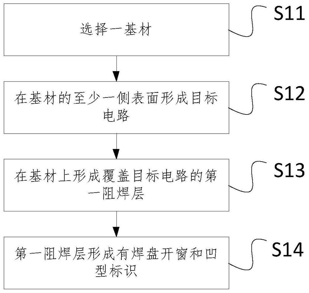
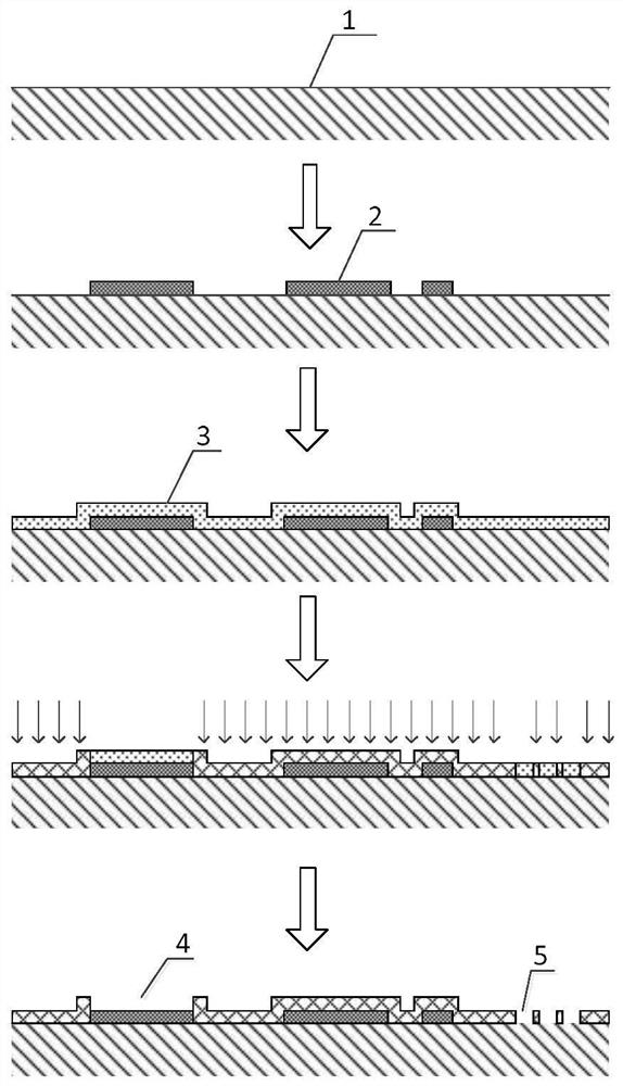
[0061] An embodiment of the present invention discloses a method for manufacturing a circuit board, comprising:

[0062] Step S21, selecting a substrate;

[0063] Step S22, using composite electronic paste to print on one side of the substrate to form a target circuit;

[0064] Step S23 , forming a first solder resist layer covering the target circuit on the side of the substrate on which the target circuit is formed;

[0065] Step S24, using a digital mask to selectively expose the first solder resist layer;

[0066] Step S25 , developing the exposed first solder resist layer to obtain solder resist openings and concave marks.

[0067] This embodiment is suitable for making a single panel.

Embodiment 2

[0069] An embodiment of the present invention discloses a method for manufacturing a circuit board, comprising:

[0070] Step S31, selecting a substrate;

[0071] Step S32, forming a target circuit by using composite electronic paste printing on both sides of the substrate respectively;

[0072] Step S33, respectively forming a first solder resist layer covering the target circuit on both sides of the base material;

[0073] Step S34, using a digital mask to selectively expose the first solder resist layer;

[0074] Step S35 , developing the exposed first solder resist layer to obtain solder resist openings and concave marks.

[0075] This embodiment is suitable for making double panels.

Embodiment 3

[0077] An embodiment of the present invention discloses a method for manufacturing a circuit board, comprising:

[0078] Step S41, selecting a substrate;

[0079] Step S42, forming a second solder resist layer on a surface of the base material;

[0080] Step S43, forming a target circuit by using composite electronic paste printing on the second solder resist layer;

[0081] Step S44, forming a first solder resist layer covering the target circuit on the side of the base material on which the target circuit is formed;

[0082] Step S45, using a digital mask to selectively expose the first solder resist layer;

[0083] Step S46 , developing the exposed first solder resist layer to obtain solder resist openings and concave marks.

[0084] This embodiment is suitable for making a single panel.


PUM


Abstract

The invention discloses a circuit board and a manufacturing method thereof, and relates to the technical field of electronic circuit manufacturing. The manufacturing process of the circuit board comprises the following steps: selecting a base material; forming a target circuit on at least one surface of the substrate; forming a first solder mask layer covering the target circuit on the substrate; and selectively exposing a partial region of the first solder mask layer, and forming a pad window for exposing the target circuit pad and a concave identifier for indicating the target circuit information on the first solder mask layer after development. According to the embodiment of the invention, the silk-screen mark and the solder resist windowing are integrally formed in a concave mark mode, so that the plate-making process is simplified, the plate-making efficiency of the circuit board is improved, and the plate-making cost is reduced.

Description

technical field [0001] The invention belongs to the technical field of rapid manufacturing of electronic circuits, and in particular relates to a circuit board and a manufacturing method thereof. Background technique [0002] As the support of electronic components, printed circuit boards provide electrical connections for electronic components. The conventional production process of printed circuit boards is generally: cutting → copper coating → etching → developing → solder mask → silk screen characters → surface treatment → Forming processing, although with the continuous iteration of the plate-making process, the current plate-making process of printed circuit boards is various, but its important plate-making links cannot be replaced, such as the solder mask process and the silk screen character process. A solder mask layer with exposed pads is formed on the circuit board to reduce the difficulty of subsequent soldering and to protect the circuit board itself, while the ...

Claims


Application Information

Patent Timeline
Patent Type & Authority Applications(China)
IPC IPC(8): H05K3/28H05K3/22H05K1/02
CPCH05K3/282H05K3/288H05K3/22H05K1/0266
Inventor 张金权尹涛
Owner BEIJING DREAM INK TECH CO LTD
Why Eureka
Try Eureka