Check patentability & draft patents in minutes with Patsnap Eureka AI!

TFT (Thin Film Transistor) array substrate structure for improving metal residues and manufacturing method of TFT array substrate structure

An array substrate structure and metal residue technology, which is applied in semiconductor/solid-state device manufacturing, semiconductor devices, electrical components, etc., can solve the problems of SD metal residue, short circuit of adjacent SD metal lines, and no improvement, and achieve the elimination of metal Residue, the effect of improving product yield

Pending Publication Date: 2022-06-28
FUJIAN HUAJIACAI CO LTD
View PDF0 Cites 0 Cited by
  • Summary
  • Abstract
  • Description
  • Claims
  • Application Information

AI Technical Summary

Problems solved by technology

[0004] In terms of manufacturing process, the existing metal layer etching methods of TFT array substrates are mainly wet etching (Mo / Al / Mo as an example) and dry etching (Ti / Al / Ti as an example). For various design requirements such as CD size accuracy, short chanel design of TFT devices, and different metal / inorganic film layer combinations, Ti / Al / Ti is often used as the metal of the SD layer, but in the actual mass production process, it will be found that on the side of the GE layer Taper Some SD metal residues will easily appear in the place, which will cause poor coverage of the post-process film stack and short circuit of adjacent SD metal lines, which will eventually affect the yield of the product.
In addition to the need to continue to improve the dry etching process in the current process, in fact, the large GE Taper (the angle of the side metal layer after the GE metal is etched) is often the main process cause of the SD metal residue, and slowing down the GE Taper is still the process. Difficulties that need to be overcome have not yet been improved

Method used


Image

  • TFT (Thin Film Transistor) array substrate structure for improving metal residues and manufacturing method of TFT array substrate structure
  • TFT (Thin Film Transistor) array substrate structure for improving metal residues and manufacturing method of TFT array substrate structure
  • TFT (Thin Film Transistor) array substrate structure for improving metal residues and manufacturing method of TFT array substrate structure

Examples


Embodiment Construction

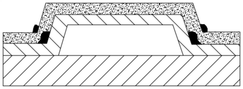
[0033] like figure 1 As shown, the present invention improves a TFT array substrate structure with metal residues, which includes a TFT side glass substrate 1, and a buffer layer 2 with grooves is arranged on the glass substrate 1, and the shape of the grooves is the upper Large and small trapezoidal shape, a GE metal layer 3 is deposited in the groove of the buffer layer, the upper surface of the buffer layer 2 and the GE metal layer 3 are flush, and the GE metal layer 3 is provided with GI insulation layer 4, the GI insulating layer 4 is provided with a PV insulating layer 5.

[0034] Further, the buffer layer 2 is usually made of SiOx, which can not only be used to planarize the glass surface, but also pattern a corresponding groove shape in a specific area.

[0035] Further, the GE metal layer 3 has low resistivity, and aluminum / molybdenum / titanium / nickel / copper / and other metals with excellent electrical conductivity and alloys such as Mo / Al / Mo or Ti / Al / Ti can be selected...


PUM


Abstract

The invention discloses a TFT array substrate structure capable of improving metal residues and a manufacturing method thereof.The TFT array substrate structure capable of improving metal residues comprises a TFT side glass substrate, a buffer layer with a groove is arranged on the glass substrate, the groove is in a trapezoid shape with the large upper portion and the small lower portion, a GE metal layer is deposited in the groove of the buffer layer, and the GE metal layer is arranged on the lower portion of the glass substrate. A GI insulating layer is arranged on the GE metal layer, and a PV insulating layer is arranged on the GI insulating layer. According to the invention, the buffer layer with the groove design is additionally arranged on the glass substrate, so that the GE metal layer is wired and deposited in the buffer layer, the CMP process is adopted, the surface of the buffer layer is flattened, the GE metal layer and the buffer layer are located on the same plane, the existence of GE taper is eliminated, and metal residues caused by the GE taper are eliminated, so that the purpose of improving the product yield is achieved.

Description

technical field [0001] The invention relates to the field of display technology, in particular to a structure of a TFT array substrate with improved metal residue and a manufacturing method thereof. Background technique [0002] IGZO is an amorphous oxide containing indium, gallium and zinc. The carrier mobility is 20 to 30 times that of amorphous silicon. It can greatly improve the charge and discharge rate of TFT to the pixel electrode, improve the response speed of the pixel, and have a more Fast panel refresh rate can realize ultra-high resolution TFT-LCD. At the same time, the existing amorphous silicon production line can be compatible with the IGZO process only with minor changes, so it is more competitive with lower temperature polysilicon (LTPS) in terms of cost. [0003] At this stage, with the obvious demand for narrow bezels of LCD displays in the market, and low-cost, high-resolution IGZO panels have gradually become a hot spot for development. The process req...

Claims


Application Information

Patent Timeline
Patent Type & Authority Applications(China)
IPC IPC(8): H01L27/12H01L21/77
CPCH01L27/1225H01L27/1248H01L27/1288H01L27/1218H01L27/1262
Inventor 陈伟陈鑫
Owner FUJIAN HUAJIACAI CO LTD
Features
  • R&D
  • Intellectual Property
  • Life Sciences
  • Materials
  • Tech Scout
  • Unparalleled Data Quality
  • Higher Quality Content
  • 60% Fewer Hallucinations
Learn More