Semiconductor device and manufacturing method thereof

A manufacturing method and semiconductor technology, applied in semiconductor devices, electric solid state devices, instruments, etc., can solve the problems of complex manufacturing process and increased cost, and achieve the effects of simple forming process, high cleanliness, and improved cleanliness.

Pending Publication Date: 2022-07-01
NINGBO SEMICON INT CORP
View PDF0 Cites 0 Cited by
  • Summary
  • Abstract
  • Description
  • Claims
  • Application Information

AI Technical Summary

Problems solved by technology

[0004] At present, the formation process of high-cleanliness cavities mainly relies on dry film or bonding process, or a combination of the two processes, while dry film materials and bonding materials are more expensive, and the manufacturing process is more complicated than other cavity processes. will also increase substantially

Method used


Image

  • Semiconductor device and manufacturing method thereof
  • Semiconductor device and manufacturing method thereof
  • Semiconductor device and manufacturing method thereof

Examples


Embodiment 1

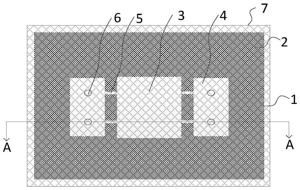
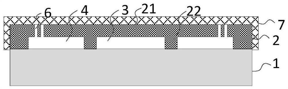
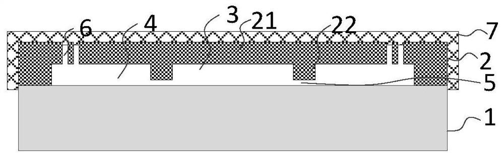
[0039] figure 1 A top view of a semiconductor device provided by an embodiment of the present invention, figure 2 for figure 1 The cross-sectional structure diagram of a semiconductor device along A-A, please refer to figure 1 and figure 2 , the semiconductor device includes:

[0040] Substrate 1, the substrate includes functional regions;

[0041] The barrier layer 2 disposed on the substrate 1, the barrier layer 2 and the substrate 1 enclose a first cavity 3 and a second cavity 4, the first cavity 3 exposes at least part of the functional area, and the second cavity 4 is located in the first cavity 3. A periphery of the cavity 3, the barrier layer 2 is provided with a release channel 5 connecting the first cavity 3 and the second cavity 4;

[0042] The barrier layer 2 is provided with a release hole 6 , the release hole 6 is located within the range of the second cavity 4 , and the release hole 6 communicates with the second cavity 4 .

[0043]The barrier layer 2 inc...

Embodiment 2

[0056] An embodiment of the present invention provides a method for fabricating a semiconductor device, and the method for fabricating a semiconductor device includes:

[0057] S01: Provide a substrate, and the substrate includes a functional area;

[0058] S02: forming a release layer on the substrate;

[0059] S03: Form a groove, the groove runs through part of the release layer or extends to a part of the depth of the release layer, and the groove surrounds the periphery of the functional area, so that the release layer in the groove and the release layer in the periphery of the groove are at least partially connected;

[0060] S04: forming a barrier layer, the barrier layer fills the trench and covers the outer surface of the release layer;

[0061] S05: A release hole is formed on the barrier layer at the periphery of the trench, and the release hole exposes part of the release layer;

[0062] S06: A first cavity is formed around the barrier layer in the trench, a seco...


PUM

PropertyMeasurementUnit
thicknessaaaaaaaaaa

Abstract

The invention relates to a semiconductor device and a manufacturing method thereof, and the semiconductor device comprises a substrate which comprises a functional region; the barrier layer is arranged on the substrate, a first cavity and a second cavity are defined by the barrier layer and the substrate, at least part of the functional area is exposed by the first cavity, the second cavity is located on the periphery of the first cavity, and the barrier layer is provided with a release channel communicated with the first cavity and the second cavity; the barrier layer is provided with a release hole, the release hole is located in the range of the second cavity, and the release hole is communicated with the second cavity. According to the invention, the second cavity is formed at the periphery of the first cavity, and the first cavity and the second cavity are communicated through the release channel, so that the release layer material forming the second cavity and the first cavity can be conveniently removed through the release hole, and the first cavity exposing at least part of the functional area is formed; the release hole is arranged on the barrier layer on the second cavity, so that the formed protective layer material is prevented from falling into the first cavity, and the cleanliness of the first cavity is further ensured.

Description

technical field [0001] The invention relates to the field of semiconductor device manufacturing, in particular to a semiconductor device and a manufacturing method thereof. Background technique [0002] With the development of semiconductor integrated circuits, the semiconductor integrated circuit manufacturing industry has become the foundation and core of the electronics manufacturing industry, supporting and promoting the prosperity and development of related industries. The cavity formation process is an important part of semiconductor devices. With the continuous progress and development of various technical fields, the types and demands of various cavities are also growing explosively, and the demand for cavities of various shapes and functions emerges one after another. [0003] Among the requirements of various cavity processes, there is a special requirement for the formation of a cavity, which requires the bottom of the cavity to maintain extremely high cleanliness...

Claims


Application Information

Patent Timeline
Patent Type & Authority Applications(China)
IPC IPC(8): B81B7/00B81C1/00
CPCB81B7/0035B81C1/00047B81C1/00055B81C1/00468B81C1/00277
Inventor 王金丽向阳辉刘孟彬
Owner NINGBO SEMICON INT CORP
Why Eureka
Try Eureka