
Systems and methods for mitigating crack growth in semiconductor die manufacturing

A crack propagation and semiconductor technology, applied in semiconductor/solid-state device manufacturing, semiconductor devices, semiconductor/solid-state device components, etc.

Pending Publication Date: 2022-07-01
MICRON TECH INC
View PDF0 Cites 0 Cited by
  • Summary
  • Abstract
  • Description
  • Claims
  • Application Information

AI Technical Summary

Problems solved by technology

However, as thinner die are formed and processed, cracks and other defects in the wafer substrate continue to appear

Method used


Image

  • Systems and methods for mitigating crack growth in semiconductor die manufacturing
  • Systems and methods for mitigating crack growth in semiconductor die manufacturing
  • Systems and methods for mitigating crack growth in semiconductor die manufacturing

Examples


Embodiment Construction

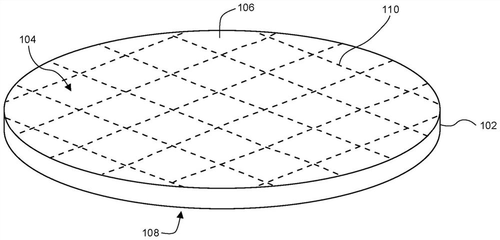
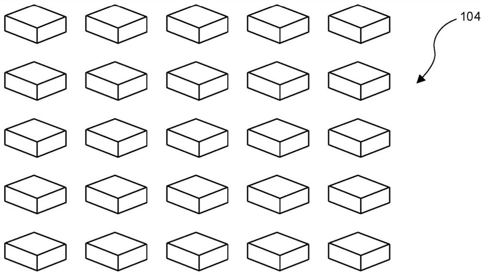
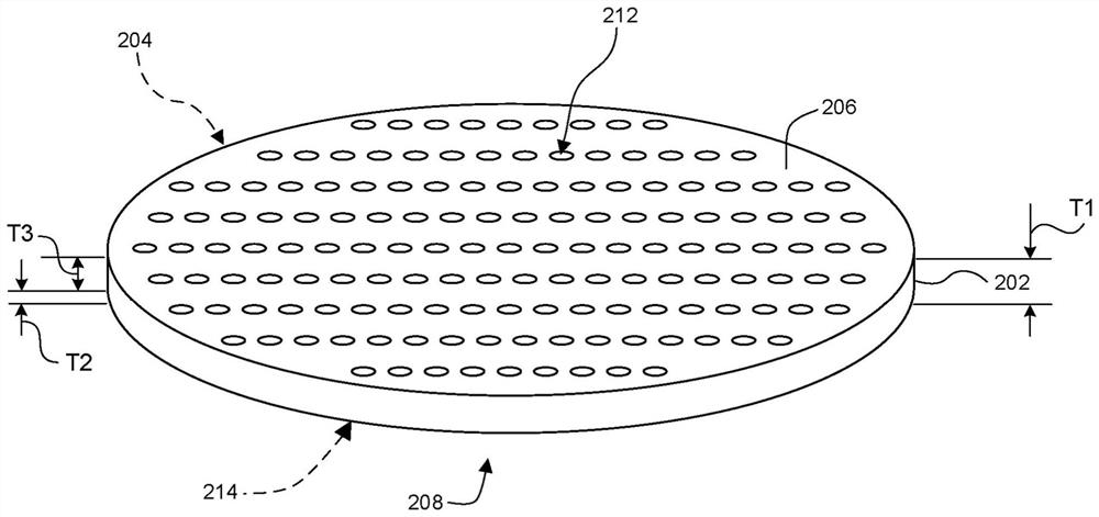
[0019] Disclosed herein is a method for mitigating crack propagation during the fabrication of semiconductor die on a semiconductor wafer, the resulting semiconductor die, and associated systems and methods. In some embodiments, the method includes forming a hole in the first side of the wafer substrate. Each hole may extend from the first side to a second side of the wafer substrate opposite the first side. The wafer substrate may have active components of the semiconductor die on the second side. The holes may extend to an intermediate depth within the wafer substrate such that individual holes have bottom surfaces that are vertically spaced from the active components. The holes are configured to mitigate crack propagation in the wafer substrate by inhibiting longitudinal propagation of the crack across the wafer substrate. In some embodiments, forming the holes may include forming the first holes in a first pattern having a first hole density, and forming the second holes...


PUM


Abstract

Systems and methods for mitigating crack propagation during semiconductor die fabrication are disclosed herein. The method includes forming a hole in a first side of a wafer substrate opposite a second side. The wafer substrate has an active component at the second side. Each aperture extends from the first side to the second side and extends within the wafer substrate to an intermediate depth such that a bottom of the aperture is vertically spaced from the active component on the second side. The hole is configured to inhibit longitudinal propagation of a crack in the wafer substrate across the wafer substrate. The method also includes back-grinding the first side of the wafer substrate after forming the hole to thin the wafer substrate. The method also includes dicing the wafer substrate after back grinding to separate the individual semiconductor dies from each other.

Description

technical field [0001] The present disclosure generally relates to methods for addressing damage to semiconductor dies. In particular, the present technology relates to methods for mitigating crack propagation during fabrication of semiconductor dies. Background technique [0002] Individual semiconductor dies are typically batch fabricated on semiconductor wafers and then divided into individual semiconductor dies. As the dimensions of individual semiconductor dies continue to shrink, batch manufacturing processes can increase throughput and reduce the difficulty of handling individual semiconductor dies. Because each wafer can contain multiple individual semiconductor dies, several steps are typically taken to protect the wafer substrate from damage. In particular, the fabrication process often includes sub-processes to protect the wafer substrate from cracking and causing other defects that can damage the wafer substrate. The cracks can destroy individual semiconductor...

Claims


Application Information

Patent Timeline
IPC IPC(8): H01L21/78H01L21/306H01L21/308H01L29/06
CPCH01L21/78H01L21/30604H01L21/3086H01L29/0657H01L23/562H01L23/28
Inventor 吴慧盈R·巴拉钱德拉恩F·斯佩蒂延斯A·L·李S·考尔S·P·科曼杜里
Owner MICRON TECH INC
Learn More