CAM-based copper surface object analysis method

An analysis method and object technology, applied in the field of copper surface object analysis based on CAM, can solve problems such as the huge influence on the manufacturing yield of copper surface objects, easy deformation of pressing, and differences in definition and description, so as to ensure the yield rate and management efficiency , Accelerate the effect of industrial upgrading

Pending Publication Date: 2022-07-05
苏州悦谱半导体有限公司
View PDF0 Cites 0 Cited by
  • Summary
  • Abstract
  • Description
  • Claims
  • Application Information

AI Technical Summary

Problems solved by technology

[0007] 1. If the proportion of the area occupied by metal copper is not enough in the manufacture of the circuit board, it will cause the board to be warped, concave and folded, and the pressure will be easily deformed.
[0008] 2 The metal contact surface area increases, heat conduction and heat dissipation
Copper laying objects are usually generated semi-automatically in CAD Layout software. However, there are differences in the definition and description of copper surface objects by various CAD software on the design side in the market, resulting in various analysis errors when they are finally merged to the CAM software on the manufacturing end. The error cost is also determined by The board factory undertakes
[0013] It can be seen that copper surface objects have a great impact on the manufacturing yield. In the past, the analysis of copper surface objects in the industry relied on the experience of engineers and the simultaneous analysis and inspection of the other four objects, which was not efficient. The industry urgently needs professional and systematic methods for copper surface objects. analysis algorithm

Method used


Image

  • CAM-based copper surface object analysis method
  • CAM-based copper surface object analysis method
  • CAM-based copper surface object analysis method

Examples


Embodiment Construction

[0044] The technical solutions in the embodiments of the present invention will be clearly and completely described below. Obviously, the described embodiments are only a part of the embodiments of the present invention, rather than all the embodiments. Based on the embodiments of the present invention, all other embodiments obtained by those of ordinary skill in the art without creative efforts shall fall within the protection scope of the present invention.

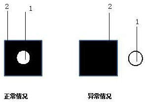
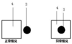
[0045] see Figure 1-3 , the embodiments of the present invention include:

[0046] A method for analyzing copper surface objects based on CAM, the steps of which include:

[0047] Step 1: Obtain or import the image graphic description file of each layer of PCB circuit board; wherein, the image graphic description file includes but is not limited to ascii-based .gerber (.gbr) file, .excellon file, Ipc2581 (.ipc) file, odb++ documents, etc.

[0048] Step 2: The CAM software calls the corresponding algorithm (or progra...


PUM


Abstract

The invention discloses a CAM-based copper surface object analysis method, which comprises the following steps of: importing an image graphic description file, analyzing and judging whether a polygonal object has risk information or not according to the type information of each object in the image graphic description file, and the like. Through the mode, the copper surface object analysis method based on the CAM microscopically ensures the yield and management efficiency of a manufacturing end, macroscopically utilizes the analysis system and method to standardly integrate upstream and downstream, accelerates industrial upgrading, and lays a way for opening a full industrial chain for full-automatic full-intelligent manufacturing of PCBs (Printed Circuit Board).

Description

technical field [0001] The invention relates to the technical field of PCB manufacturing, in particular to a method for analyzing copper surface objects based on CAM. Background technique [0002] CAM defines five types of objects (feature): 1. Line object (Line), 2. Arc object (Arc), 3. Pad object (Pad), 4. String object (Text), 5. Copper surface Object (Surface). In a broad sense, all objects on the circuit board are copper objects, but at the computer-aided manufacturing (CAM) level, a narrow copper surface object (Surface) is redefined. [0003] The description of copper surface objects in CAD software is as follows: It is a polygonal outline described by multiple points, and then filled into a surface. [0004] Reasons for copper-clad objects [0005] Generally speaking, we can intuitively understand that in the whole circuit, the three objects of straight line, arc and pad can ideally describe the circuit, while the string object is only for the marked graphics and ...

Claims


Application Information

Patent Timeline
Patent Type & Authority Applications(China)
IPC IPC(8): G06F30/392G06F30/398G06F115/12
CPCG06F30/392G06F30/398G06F2115/12
Inventor 王克昌严启晨
Owner 苏州悦谱半导体有限公司
Why Eureka
Try Eureka